Automated optical inspection (AOI) is one of the best inspection tools in the SMT environment. It helps identify issues and defects in the early stages of the manufacturing process. This article discusses AOI and its applications in the PCB industry.
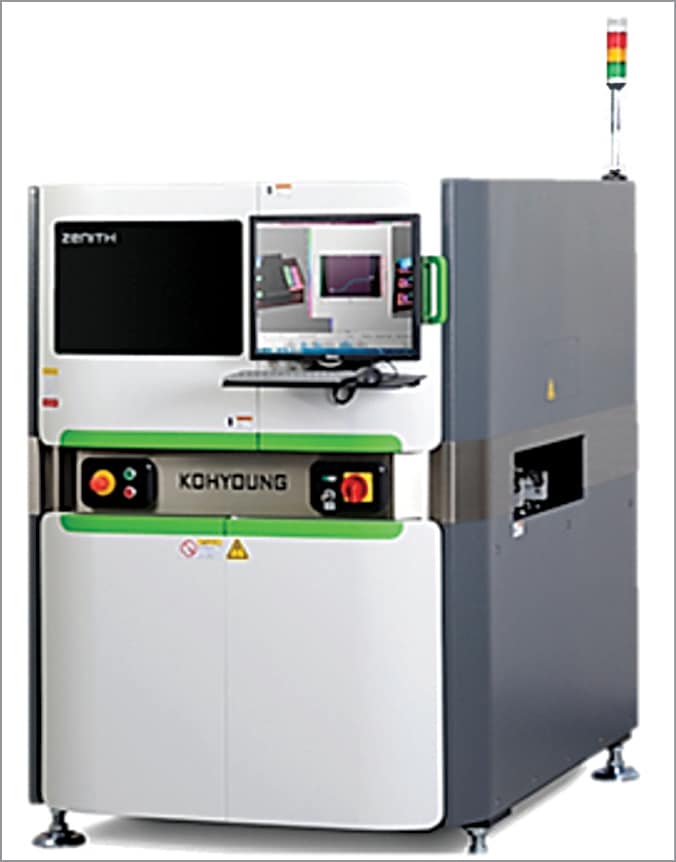
The rapid development in the semiconductor industry towards miniaturisation has promoted an apparent change in the printed circuit board (PCB) technology. As a result, the number of pin counts has increased in integrated circuits per unit area. The density of components, track width, and spacing between bonding pads are becoming smaller and smaller. Component pad design, selection of solder paste, and solder volume per pad for good solder joint have become a vital part of electronic PCB assembly production lines.
Further, due to the tremendous increase in production volumes and quality expectations, the process of inspection has become an essential part of the surface-mount technology (SMT) environment. The industry has adopted the concept of scientific and data-driven methodology for quality analysis and improvement. The conventional concepts of sampling inspection, manual visual inspection, and tool-based inspection were not the solution for high-density PCB assembly products. As a result, process engineers and quality control engineers are turning to automated machines for addressing quality and productivity issues.
Hence, machines for solder paste inspection (SPI), automated optical inspection (AOI), flying probe test, and automatic X-ray inspection have become an important part of PCB assembly manufacturing industry. This article discusses automated optical inspection (AOI) and its applications in the PCB industry.
Why AOI?
Why inspection, tests, and measurements are important during the manufacturing process? The answer is simple—cost reduction. It’s crucial to identify issues and defects in the early stages. Any small defect in terms of component placement, lead solder bond, and component functionality can lead to drastic repair cost and field failures. Manufacturers and assemblers prefer high-quality assemblies to ensure no defects.
Automated optical inspection (AOI) is one of the best inspection tools in the SMT environment. Though automatic X-ray inspection is the latest trend, AOI is the most cost-effective and reliable inspection tool. By using one or more HD cameras, this process captures images of assembled PCB surface with the help of a light source. It then compares the captured scanned images with pre-existing template images to detect both catastrophic failures (for example, missing component) and quality defects.
AOI applications
AOI can be applied to both bare board PCBs and PCB assembly lines. Generally, post-reflow AOI is preferred by many process engineers depending on what type of information you are looking for and how fast the inspection needs to be completed.
In the broad sense, AOI must be capable to inspect the presence of an object, recognise barcode information, perform measurement or gauging, package dimension, and lead condition to generate yield rate, distributed defect type, the number of defects, etc.
The following information can be expected from the inspection results:
- Body of machine missing
- Body dimension
- Polarity
- Upside down
- Tombstone
- Billboard
- Pad offset or shift
- Coplanarity
- Solder fillet
- Missing lead
- Bridging
- Markings
Fundamentals of AOI
The core structure of the automatic optical inspection system includes a CCD image system, AC servo control x, y workbench, and image processing system. In other words, the CCD image system, AC servo control x, y workbench, and image processing systems are the core of AOI. The actuating parts (drivers and axis), image grabbing system (sensors, optical and illumination), and software processing part work in close relationship to each other, so the speed of each must be synchronised.
With the development of digital computing, machine vision and image processing have become essential to automate the inspection process with the help of high-resolution cameras, lighting devices, illumination techniques, and an efficient processing algorithm.
The faster the processor, the less time the machine vision system will need to process image information. Speed is an important factor for high-volume production lines. Also, specific inspection software is available as per specific needs.
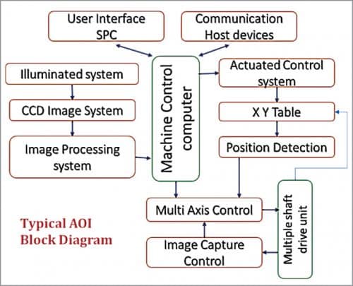
The block diagram of the AOI system is given in Fig. 2. This is the same for solder paste inspection. The only difference is light source or illumination and processing software. These machines differ in terms of the height they need to measure. SPI measures the height of solder paste, whereas AOI measures the height of components. Therefore AOI has a four-way or eight-way projection, while SPI is provided with a two-way or four-way projection.
Illuminated system
For any type of camera, enough light means a guaranteed good image. Lighting is important because it illuminates the part to be inspected. Many types of lighting sources such as fluorescent tubes, UV tubes, strobe lamps, high-intensity halogen lamps, and LED lamps are being used in the electronics industry for the best illumination.
Currently, many AOI manufacturers are using LED lamps and IR-RGB LED dome styled illumination. The choice of a light source depends on what you want to inspect. The lighting system generally includes white, red, green, and blue lights in a configurable lighting module. Machine vision systems need to carefully control lighting or adjust light intensity to ensure accurate and repeatable results by using digital controllers. The angle of lighting is also important because taller components in PCBA block the light from reaching smaller components.
Hence, the latest AOI machines are equipped with one or more projections from different angles to offer the best overall illumination. Also, the selection of the type of light and the location at which the light source is fixed matters a lot.
CCD image system
Typically, five components make the machine vision system (Fig. 3).
- Lighting
- Lens
- Image Sensor
- Vision processing or image processing
- Communication
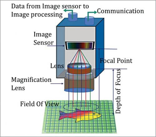
Lighting illuminates the part to be inspected. The lens captures the image and presents it to the sensor in the form of light. The image sensor converts light into a digital image, which is then sent to processing unit for analysis.
Image processing follows a process to review the image and extracts the required information as per the interest of the user. Finally, the resulting data is communicated as per the user’s interest.
Before proceeding further into the vision camera, let us review some fundamentals about the industrial vision system.
Fundamentals of vision system
All AOI original equipment manufacturers (OEMs) provide specifications about their products. Let us consider an example of such specification related to vision performance (Fig. 4).
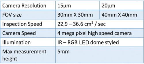
It is very important to understand the meaning of each parameter to visualise the capability of AOI.
AOI process starts with a digital image. Capturing an image or picture represents a scene. Here picture/scene means it is a combination of object +shape+background (Fig. 5). The quality of the picture depends on brightness, sharpness, and clarity.
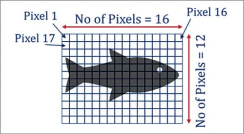
- Pixel=Picture+element
- Resolution=Number of pixels/inch
- Pixel dimension=16×12 pixels
- Pixel density=16 pixels/inch= Resolution
In digital language, a picture is a matrix of pixels. A pixel can be defined as the smallest element in a picture, which means the smallest unit of the entire image. Each pixel location represents a row and column. Each pixel contains information on light intensity level measured in grayscale for black and white, or red, green, and blue values, or a combination of the three colours. This is the reason why the lighting system and lens play a vital role in defining the quality of a pixel or the amount of information in a pixel.
Image sensor
The image sensor is the heart of the camera. It is important to ensure that camera has the right sensor resolution for your application.
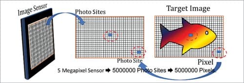
The image sensor is made up of a large number of squares called photo sites. Each photo site corresponds to pixels in an image. So, if you say 5MP pixel camera, it means it produces an image using 5,000,000 pixels, which in turn will have 5,000,000 photo sites in its image sensor. In practical applications, if an industrial camera specifies its frame size as 2560×2048 pixels, it means a pixel density of 5,242,880. In short, it means five megapixels.
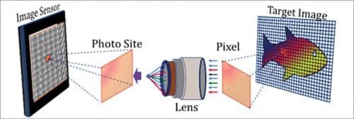
Image sensor properties. Fig. 8 shows how pixel information is converted into an image. Light energy is assumed as illumination reflected from the pixel, that is, photon energy captured by the camera lens. The individual pixel information is absorbed by the respective photocells in the sensor. The camera sensor converts incoming photon energy into electrical charges, which are then further processed to generate images.
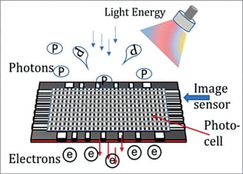
The number of electrons you get for the number of photons is called quantum efficiency.
- The higher the quantum efficiency, the more is the information available in an image.
- The size of the pixel is proportional to the quality of light collected.
- The bigger the sensor, the higher the image quality. The number of pixels besides their size also plays an important role.
Types of sensors
A charge-coupled device (CCD) is an integrated circuit containing an array of linked or coupled capacitors. Under the control of an external circuit, each capacitor can transfer its electric charge to a neighbouring capacitor. CCD sensors are a major technology used in digital imaging. In a CCD image sensor, pixels are represented by p-doped metal-oxide-semiconductor (MOS) capacitors. These MOS capacitors, the basic building blocks of a CCD, are biased above the threshold for inversion when image acquisition begins, allowing the conversion of incoming photons into electron charges at the semiconductor-oxide interface
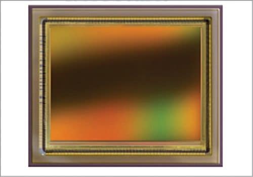
Complementary metal oxide semiconductor (CMOS) uses complementary and symmetrical pairs of p-type and n-type MOSFETs for logic functions. CMOS technology is used for constructing integrated circuit (IC) chips, including microprocessors, microcontrollers, memory chips (including CMOS BIOS), and other digital logic circuits. It has replaced the earlier transistor-transistor logic (TTL) technology. It is powerful, sensitive, fast, and affordable. In this, electron to voltage conversion happens at individual pixel itself because an extra circuit added to each pixel pushes out a single charge parallelly and generates an image.
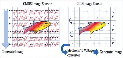
In both CCD and CMOS cases, pixel information, in the form of light from the camera lens, is filtered through colour filters to disperse in red, blue, green, and white colours in the sensor.
- The more the light or photons, the brighter is the pixel. The brighter the pixel, the higher is the digital value. This digital value is described as a gray value.
- For a colour image, we need colour values for each individual pixel in an array. First, the array recognises the gray value (red, green, and blue) and calculates colour for each pixel from the gray value and then incorporates colour for the whole image.
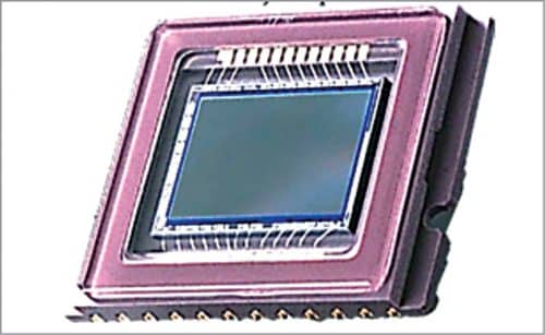
Coming back to SMT technology, a picture is an image with an illustration of pixels. The quality of the image is usually expressed in microns.
The performance and capability of AOI depend on the choice of the light source, digital camera capability, speed of image acquisition, and data capture ability. The design and technology adopted with respect to camera specifications, illumination system, image capture, and processing differ from manufacturer to manufacturer.
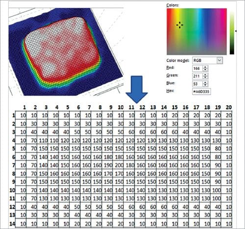
Image processing system
The image processing system is purely based on the capability of the vision system and mechanism for extracting the information required in an application. In the majority of industrial applications, especially in AOI, the processing of images takes place externally through the PC base system. This process is performed by dedicated software with a wide variety of interfaces and tools.
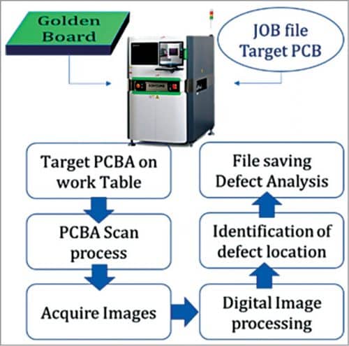
This software performs several steps or algorithms. It acquires image from the sensor, preprocesses to optimise the image, analyses according to features, sets the geometry and tolerance as per inspection conditions, and finally, results are communicated to the user in a defined format.
There are two types of technology-based AOI available in the market—Image-based AOI and algorithm-based AOI. The inspection process is different for both the technologies. Image-based AOI is quite popular, whereas algorithm-based AOI is preferred only in some applications and is quite expensive.
AOI programming
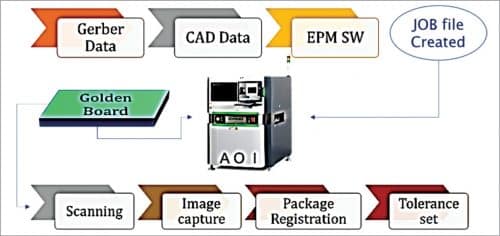
Creating a job file is the key to product programming. Here Kohyoung AOI machine is considered as an example to know the steps involved to create a job file. The creation of a job file is essential for AOI inspection as we need to assign detailed information such as package size and inspection area for every component. Here are the steps to create a job file for a target production PCB assembly model (Fig. 15).
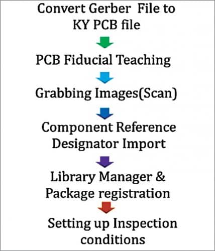
The basic information needs to be provided to the AOI machine through Gerber data (image file) and CAD data (placement data) to create a KY PCB file so that the machine can understand/read this PCB file. Machine EPM software collects the details about PCB size, masking area, footprints, arrays, and fiducial data. Gerber and CAD data is imported to create a PCB file as the first step of programming.
Target PCB is placed on conveyor to perform board level teaching—Fiducial, bad mark, and barcode. Once board-level teaching is defined, the images of the target PCB are grabbed through scanning. This scanning process is mandatory. Lots of real images must be combined with KY PCB data to get more precise information for each component.
The next step is to import the CRD file from CAD data to assign component reference designation (CRD), that is, package type, part number, x, y, and angle information.
Before setting up inspection conditions, package information (package type and size) must be registered in the library manager. This is the most important element for 3D inspection. The basic function is the separation of the mapped and unmapped components. Inspection conditions are nothing but user-defined tolerance limits so that acceptance criteria are defined with respect to specification limits.
All component information and relevant inspection conditions are saved in the job file as the final step.
3D inspection
3D inspection is nothing but an extended optical inspection system with measuring capability. Solder fillet, coplanarity, tombstone, and IC lift are the inspection parameters that can only be measured by 3D because height measurements are difficult to detect with the 2D inspection method. High dynamic range 3D inspection technology extracts the shapes of components and solder joints and detects all types of defects.
The quality of the solder joint can be inspected and determined from the geometric and optical properties of solder meniscus. These parameters determine the reflection properties of the meniscus formed by the solder joint. Inspection equipment measures the solder fillet (dry solder on the pad, excess solder, and insufficient solder on the pad) reflection pattern with the help of an image processing algorithm. Hence, AOI uses high-resolution cameras to detect defects in the micrometre (µm) scale.
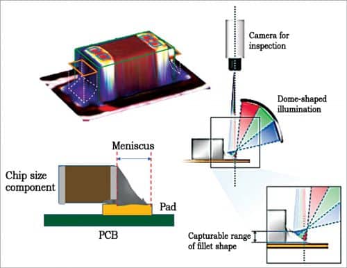
Several optical measuring techniques are used in this process, such as:
- Laser triangulation
- Fringe pattern analysis
- Shape from shading
- Phase measuring
- Moire topography
Moire technology, fringe pattern, and phase measuring technologies are well adopted by AOI OEMs for their 3D component assembly inspection. Further, to avoid shadow and diffusion problems, they use patented technologies and solve projection obstacles by using four- or eight-way light projections for better image capture for all PCB configurations.
Summary
Compared to AOI, AXI is a newly developed inspected method. X-ray inspection makes the solder joint so direct and clear. Solder joint defects are automatically inspected through an image analysis algorithm. But AOI is a less expensive and cost-effective solution and ideal for post reflow. But in some cases, especially in RF products manufacturing, pre-reflow AOI is a widely preferred inspection process.
Currently, AOI uses fast industrial cameras that can grab up to 250 frames/sec by using 5MP CMOS sensors with remarkable image quality for high-speed applications. The improved version of AOI provides a high signal-to-noise ratio, low light performance, sharper images, and accurate colours.
AOI OEMs also consider brightness, sharpness, quantum efficiency, sensor and pixel size, resolution, dynamic range, signal to noise ratio, and contrast, which clearly differentiates between good and bad images.
Adibhatla Krishna Rao is currently working with NMTronics India Pvt Ltd. He has over 26 years of experience in the SMT manufacturing and service industry


