
Energy shortage and clean water scarcity are two key challenges for global sustainable development. The concept of simultaneous production of clean water and electricity by solar energy has been recently investigated by several groups.
The world is on the verge of a water crisis. Rainfall shifts caused by climate change plus escalating water demands of a growing world population threaten society’s ability to meet its mounting needs. By 2025, the United Nations (UN) predicts that 2.4 billion people will live in regions of intense water scarcity, which may force as many as 700 million people to travel a long distance from their home in search of water by 2030.
These water woes have made people thirstily eye the more than one sextillion litres of water in Earth’s oceans, saline lakes and some underground aquifers with high salt content as a source of drinking water after desalination. (Desalination is necessary to make saline water fit for drinking or irrigation.)
India has sixteen per cent of the total world population, but only four per cent water resources. Seventy per cent of Rajasthan is arid, and 31 per cent of its groundwater and many lakes are saline. It is estimated that sixty per cent of the area in Rann of Kutch in Gujarat contains native saline water. And there is extreme water scarcity in Chennai due to negligence of water governance. These are just a few places that require installation of desalination plants urgently.
Technology overview
A device that can produce electricity from sunlight while simultaneously purifying water from sea/polluted water has been invented by researchers. This invention can solve two problems in one stroke—the device is not only a source of green energy but also offers a cheaper alternative to current technologies for purifying water.
Conventional technologies often consume large amounts of electricity and require infrastructure beyond the reach of many communities that lack basic access to safe drinking water—a situation thought to affect more than 780 million people worldwide. These people, it has been estimated, spend a collective 200 million hours each day to fetch water from distant sources.
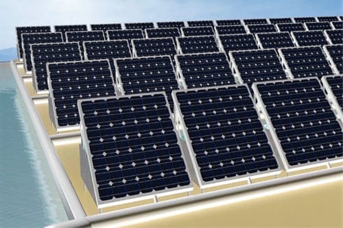
With solar farms often located in arid regions, the new device could provide clean water where it is needed the most. It could even be installed by an individual in the backyard. By having significant amount of fresh water produced continuously on daily basis many challenging tasks can be easily achieved.
The generated clean water can be used for drinking, farming, cleaning solar panels and making desert farming possible, while waste water after cleaning can be used for growing grass below the solar panels to be consumed by livestock. By combining two types of devices, which typically require a large land area each, the system becomes simple and compact. General arrangement of dual-purpose photovoltaic (PV) cells is shown in Fig. 1.
Simultaneous production of fresh water and electricity has been achieved by an integrated solar PV panel – membrane distillation (PV-MD) device. In a typical solar cell, eighty to ninety per cent of absorbed solar energy is undesirably converted to heat and then it is passively and wastefully dumped into ambient air.
PV cells are protected by glass and held together in a metal frame. These are comparable to materials that make up windows and frame of a car. When a car is parked in a parking lot on a hot summer day, it gets extremely hot, but there is little danger of it burning. PV cells can get as hot as 65°C in the summer if there is no proper ventilation. PVs are generally tested at 25°C and rated at that temperature. If a panel is rated to have a temperature coefficient of 0.50 per cent per degree Celsius, then PV power will decrease by half a per cent every degree the temperature rises above 25°C.
In the laboratory it has been found that, when a PV panel reaches maximum allowable temperature of 45°C, air cooling by a fan decreases the temperature by 4.7°C and, hence, efficiency is increased by 2.6 per cent. But if the same panel is cooled by heat pipes using water as in MD, temperature reduces by 8°C and PV efficiency increases by more than three per cent.
By mounting a water distillation system on the back of a solar cell, engineers have constructed a device that doubles as an energy generator and water purifier. While the solar cells harvest sunlight for electricity, heat from the solar panels drives evaporation in the water distiller below. Vapour wafts through a porous polystyrene membrane that filters out salt and other contaminants, allowing clean water to condense on the other side. This does not affect electricity production and at the same time gives fresh water, deemed safe without dissolved salts, suspended materials and free from any bacteria, as bonus.
Selection of PV module
Crystalline solar cells have dominated the PV market since the 1950s. Silicon is non-toxic and abundantly available in Earth’s crust. Silicon PV modules have shown long-term stability over decades.
Silicon solar cells are getting cheaper with time, too. Main factors contributing to this decrease in price are efforts to develop new methods and interesting designs of cell architecture, growing automation of factories and use of diamond wire saws to cut silicon wafers, thereby reducing the cutting loss of costly silicon ingot.
Finally, cell manufacturing equipment are becoming increasingly efficient, reducing power consumption. At present, price of modules is about US$ 0.30 per watt DC, which is speculated to fall to US$ 0.18 per watt DC in the next five years—a forty per cent drop.
There is not much difference in price between imported and Indian solar panels. At present in India, just the panel costs about ` 45 per watt of peak power generated for monocrystalline cells, ` 30 per watt for polycrystalline cells and ` 25 per watt (approximately) for amorphous silicon cells.
There are mainly three types of silicon solar cells, as explained below and shown in Fig. 2.
Monocrystalline silicon solar cells. These solar cells are made from a very pure type of silicon. Monocrystalline cells are cut from a silicon ingot grown from a single large crystal of silicon. The higher the purity, the better the alignment of the molecules, making the device more efficient at converting sunlight into electricity.
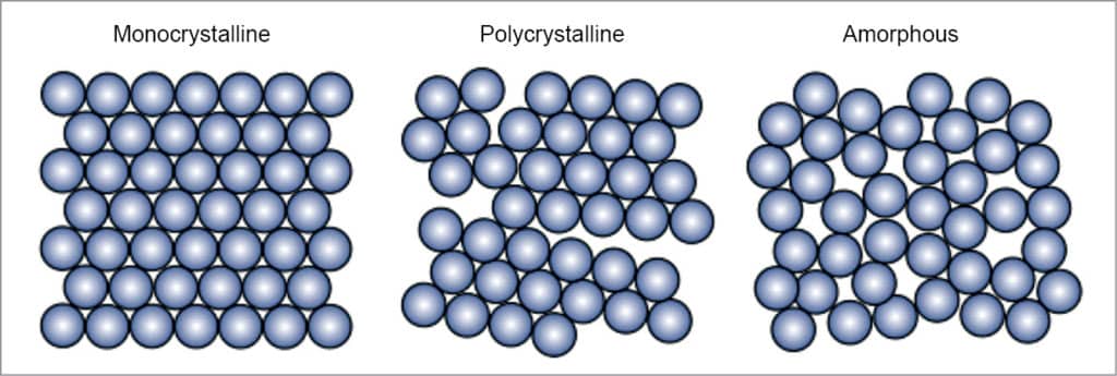
Monocrystalline solar cells are the most efficient of all. Their efficiencies have been documented at upwards of 20 per cent (25 per cent maximum in a laboratory). These also last the longest, more than 25 years, but these are the most expensive, too. One of the reasons why these are expensive is that the four-sided cutting process ends up wasting a lot of silicon, sometimes more than half.
Polycrystalline silicon solar cells. These solar cells are cut from cast square ingots made by melting many smaller crystals. Liquid silicon is poured into blocks, which are cut into thin plates. This way these are made much more affordable since hardly any silicon is wasted during manufacturing.
Because there are many crystals in each cell, there is less freedom for electrons to move. As a result, these cells have lower efficiency ratings than monocrystalline panels. These cells are large—a factor that must be considered if there is a space constraint. On average, conversion efficiency is between 14 and 16 per cent with laboratory records over 21 per cent.
Another drawback is that these cells have lower heat tolerance. Their life is more than twenty years.
Amorphous silicon solar cells. The word amorphous means shapeless. Amorphous silicon is the non-crystalline form of silicon. Amorphous silicon panels are formed by vapour—depositing a thin layer of silicon material (about one micrometre thick) on a substrate material such as glass, metal or plastic at temperature as low as 75°C. These are either tandem or triple-layer systems that are optimised to capture light from the full solar spectrum. These are cost-competitive. Since amorphous silicon is full of natural defects, its efficiency is low, about seven to eight per cent. Life is estimated to be more than fifteen years.
As efficiency of polycrystalline solar cells is reasonable, these have a long life and low price. These solar cells are most suited for dual-purpose applications, provided there are no space constraints.
Morphology of PV device
Light is made of tiny particles called photons. A beam of sunlight is like a bright yellow fire hose shooting trillions upon trillions of photons in its way. If a solar cell is kept in its path, it catches energetic photons. These photons strike electrons in the silicon which are ejected, resulting in the formation of holes—vacancies left behind by escaping electrons.
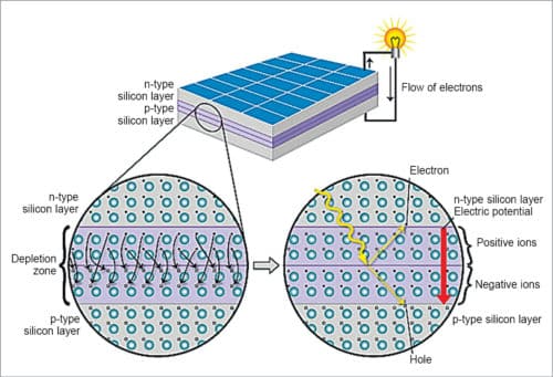
If this happens in an electric field, the field moves the electrons to n-type layer and holes to p-type layer. When n-type and p-type layers are connected with a metallic wire, electrons travel from n-type layer to p-type layer by crossing the depletion zone and then going through an external wire at the back of n-type layer, creating a flow of electricity (Fig. 3).
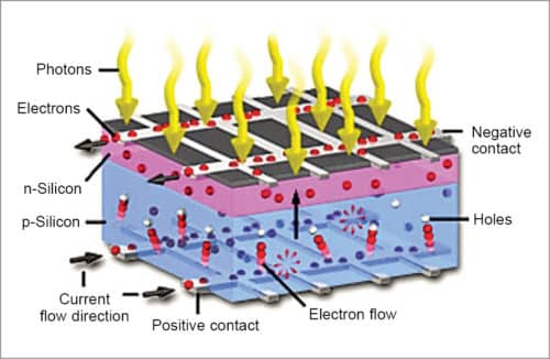
A solar cell consists of a layer of p-type silicon placed next to a layer of n-type silicon. In n-type layer there are excess electrons; and in p-type layer there are excess positively-charged holes. The n-type silicon is made by including atoms that have one more electron in their outer level as compared to silicon, such as phosphorus.
Phosphorus has five electrons in its outer level while silicon has four electrons. It bonds with its silicon neighbour atoms, but one electron is not involved in bonding. Instead, it is free to move inside the silicon structure. The p-type silicon is produced by adding atoms, such as boron or gallium, that have one less electron in their outer energy level than silicon. Because boron has one less electron than is required to form bonds with the surrounding silicon atoms, an electron vacancy or hole is created.
When these two materials are placed side by side inside a solar cell, n-type silicon’s spare electrons jump over to fill the gaps in p-type silicon. This means, n-type silicon becomes positively-charged and p-type silicon becomes negatively-charged, creating an electric field across the cell. Near the junction of the two layers, electrons on one side of the junction (n-type layer) move into the holes on the other side of the junction (p-type layer). This creates an area around the junction, called depletion zone, in which electrons fill the holes, as shown in Fig. 4.
Because silicon is a semiconductor, it can act like an insulator, maintaining imbalance. As photons smash electrons off silicon atoms, this field drives them along in an orderly manner, providing electric current in the external circuit.
Anatomy of a polycrystalline solar cell
Fig. 5 shows a typical cross-section of a solar cell. An optimum silicon solar cell with light trapping and very good surface passivation is about hundred micrometres thick. However, thickness between 200 to 500 micrometres is typically used, partly from practical considerations such as making and handling thin wafers with ease and for surface passivation reasons.
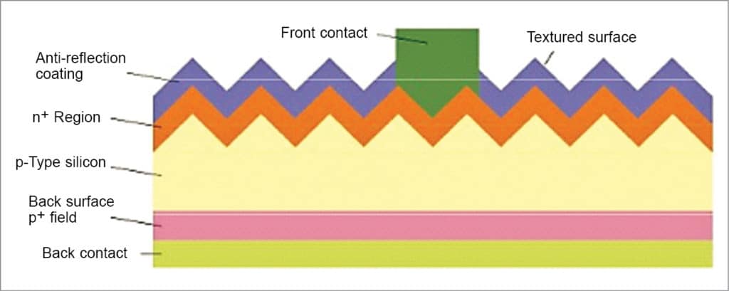
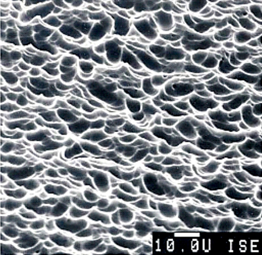
The front side of a PV cell is textured with a few micrometres of standing, round-shaped valleys, as shown in Fig. 6, to increase the amount of light coupled to the cell. Functions of the texture are to increase transmission of incoming photons into the silicon absorber and to increase the path length of photons inside the absorber.
As shown in Fig. 5, the front side is further coated with 75-nanometre-thick hydrogenated silicon nitride with a refractive index of 2.1, enabling reduction of front reflection. Fig. 5 also shows that, at the front side, front contact of continuous H-like pattern of a thin transparent silver conductor is formed from sintered silver paste that penetrates into silicon to a depth of thousand nanometres for efficient carrier transport and connected to busbars for collection of current.
The front-side top layer is doped with phosphorus to form a p-n junction, enabling diffusion of a minority carrier (hole) within the layer and to allow sufficient conduction to enable efficient transport of majority carriers (electrons) to the contact. The rear side is fully metallised with aluminium, alloyed with silicon, with contact pads connected to the busbar for efficient carrier transport. The alloying process produces a layer of silicon heavily doped with aluminium, which reduces the recombination rate at the rear end.
The PV-MD process
Recently, scientists have fabricated a PV-MD device that can stably produce more than 1.60 kilograms of clean water per hour per square-metre of PV surface from sea water, while simultaneously generating electricity with an efficiency of more than eleven per cent under one Sun irradiation. Its high clean water production rate is realised by constructing a multi-stage membrane distillation (MSMD) device at the back of the solar cell to recycle the latent heat of water vapour condensation at each distillation stage. This composite device can significantly reduce capital investment costs by sharing the same land and the same mounting system.
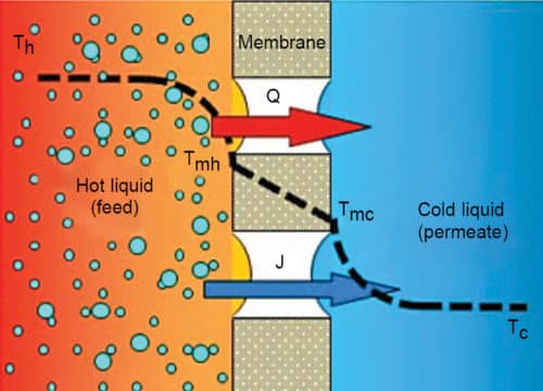
Membrane distillation is a thermal separation process that can be used for extraction of clean water. Mass transfer occurs through a porous membrane, which cannot be wetted for the solvent. Two liquids with different temperatures contact the membrane. On input side (feed side), it is the warm aqueous solution, for example, sea water; and on effluent side (distillate side), it is condensed steam diffused through the membrane.
Feed temperatures in MD typically range from 40°C to 85°C. The driving force in MD is the partial pressure difference between each side of the membrane pores. Temperature difference between the two liquids leads to vapour pressure difference across the membrane. Due to the hydrophobic nature of the membrane, only vapour can pass across the membrane, and not any liquid solution being distilled (Fig. 7).
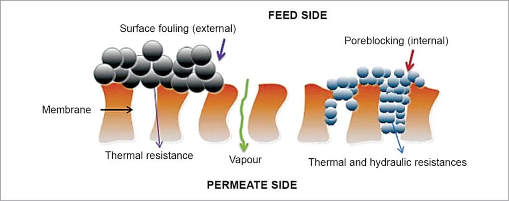
Membranes should be hydrophobic and micro-spongy. These are mostly produced from polytetrafluorethylene (PTFE), pollypropylene (PP) or polyvinylidene-fluoride (PVDF). Pores must be large enough to allow mass flow, but small enough to prevent intrusion of water under operating conditions. Membranes with pore diameter of 0.01mm to 1.00mm can be used for membrane distillation. Whenever salts are accumulated on the membranes, as shown in Fig. 8, the same should be removed by washing.
MD is a separation process that could operate with minimum external energy requirements and least capital and land for the plant. Required equipment for this process are much smaller, which translates to savings in terms of real estate. Operating temperatures are much lower because it is not necessary to heat the process liquid above its boiling point. These benefits result in less heat loss to the environment through the equipment surface. Therefore low-grade waste heat energy source like solar, geothermal energy and waste heat from industrial plants can be coupled with MD system.
In fact, MD plants powered by waste heat of PV cells are cost-competitive with RO process for clean water production. Easier operating conditions, lower safe operating pressure at ambient conditions and lesser fouling problems are other benefits. MD process is a very efficient salt removal system from raw sea water by reducing its input salinity from ~25,500mg/l TDS content to 9mg/l TDS.
In case MD-produced water is to be used as drinking water, direct addition of certain minerals that are needed by our body must be added to the clean water as per WHO standards.
The solar cell harvests short wavelength sunlight to generate electricity. Large amount of waste heat is simultaneously generated as a side-effect from two pathways. The first one is relaxation of short wavelength sunlight-excited electrons, and the second pathway is photothermal conversion of long wavelength sunlight. In a typical solar cell, eighty to ninety per cent of absorbed solar energy is undesirably converted to heat. Waste heat is dumped into ambient air as waste. Using this concept, waste heat is considered as a resource and utilised to power PV-MD devices to produce clean water.
Fig. 9 shows the arrangement of an integrated PV-MD device. Commercial polycrystalline silicon solar cell is used both as an electricity generator and as a photothermal component. PV-MD device is constructed at the back of the solar cell for clean water production. To reduce heat loss into the atmosphere, sides of the composite device are sealed by polyurethane foam with low thermal conductivity.
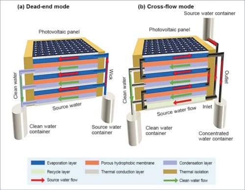
Each stage of the MSMD device has four separate layers:
- Top thermal conduction layer
- Hydrophilic porous water evaporation layer
- Hydrophobic porous layer of MD membrane for vapour permeation
- Water vapour condensation layer
Aluminium-nitride (AlN) plate is used as the thermal conduction layer due to its very high thermal conductivity and its anti-corrosive nature to saline water. The hydrophobic porous layer is made from polystyrene (PS) membrane. Water evaporation and condensation layers are composed of the same material—commercial hydrophilic quartz glass fibrous (QGF) membrane with non-woven fabric structure.
In each stage of the MSMD device, heat is conducted through the thermal conduction layer to the underlying hydrophilic porous layer. Source water inside the hydrophilic porous layer is thus heated to produce water vapour. Water passes through the hydrophobic porous membrane layer and ultimately condenses on the condensation layer to produce clean water. The driving force behind water evaporation and vapour condensation is the vapour pressure difference caused by the temperature gradient between evaporation and condensation layers.
In each stage, latent heat of water vapour, which is released during condensation process, is utilised as the heat source to drive evaporation in the next stage. The multi-stage design ensures that heat can be repeatedly re-used to drive the water evaporation and condensation cycle, which sets up an upper theoretical ceiling for the clean water production rate of ~1.60kg/m2 per hour, under one Sun condition in such a system.
The system can be operated either in dead-end mode, as shown in Fig. 9(a), where all fluids flow in parallel. Here, source water is passively wicked into the evaporation layer by hydrophilic QGF membrane strips via capillary effect. In this case, salt concentration in the evaporation layer keeps increasing till it reaches saturation. But this mode requires washing to remove accumulated salts inside the device.
The system can also be operated in cross-flow mode, as shown Fig. 9(b), where source water flows into the device driven by gravity or by a pump, and flows out of the device before reaching saturation. Here, outgoing water flow takes away a small amount of sensible heat, leading to a slight drop in clean water productivity in the earlier stage. However, it solves the problem of salt accumulation and avoids the need for frequent cleaning, which makes the device suitable for continuous long-term operation.
Rathindra Nath Biswas is a 1964-batch chemical engineering graduate from Jadavpur University, Calcutta. He was awarded a certificate for designing Benzol Plant by Giprokoks, USSR, and Certificate of Honour by Indian Institute of Metals. He has published 35 research papers in various journals. He retired from service as head – MECON, Durgapur.