





Atomically thin MoS₂ transistors with sub-5nm channels have demonstrated switching beyond silicon’s theoretical limits, pointing toward smaller and more energy-efficient chips for future computing.
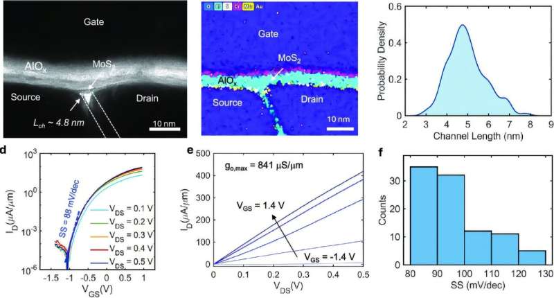
Researchers at Carnegie Mellon University have demonstrated molybdenum disulfide (MoS₂) transistors with channel lengths below 5nm that overcome a key scaling limitation of conventional silicon devices. The transistors showed subthreshold switching performance beyond the theoretical silicon limit at comparable dimensions, highlighting the potential of two-dimensional semiconductors for future chip technologies.
The work addresses one of the major problems that emerges as silicon transistors become extremely small. As the channel shrinks, the gate finds it increasingly difficult to completely control current flow. This can allow electrons to leak through even when the transistor is switched off, increasing power consumption and limiting further scaling.
MoS₂ offers an alternative because its atomically thin structure can provide better electrostatic control at very small dimensions. However, simply replacing silicon with a two-dimensional material does not automatically deliver better transistor performance. The researchers therefore co-designed the semiconductor material, device structure, and fabrication process.
The key features are:
- Sub-5nm physical channel length
- Atomically thin 2D MoS₂ semiconductor
- Air-gap structure for improved gate control
- Reduced leakage at nanoscale dimensions
- Demonstrated fabrication across a 4-inch wafer
A key feature of the demonstrated device is an air gap beneath the transistor channel. This structure improves the gate’s ability to control the channel and suppress unwanted current leakage. Better gate control becomes increasingly important as transistor dimensions approach the nanometre scale.
The team also demonstrated that the technology can move beyond isolated laboratory devices. MoS₂ transistors were fabricated across a 4-inch wafer, indicating a possible pathway toward wafer-scale processing rather than limiting the technology to individual experimental devices.
The demonstration could be significant for processors and other high-density electronics, particularly as computing workloads such as AI demand greater performance within tight power budgets. Smaller transistors could potentially allow more devices to be integrated into a given area while reducing some of the leakage-related limitations associated with aggressively scaled silicon.
However, the technology is not yet ready for commercial chip production. Further work is required to improve fabrication, integration, reliability, and manufacturing compatibility. The research nevertheless suggests that continued transistor scaling may depend not only on shrinking silicon devices but also on combining new semiconductor materials with new device architectures.

