How can semiconductor inspection keep pace with complex packaging? An acoustic system combines high-resolution imaging with faster scanning and automated defect analysis.
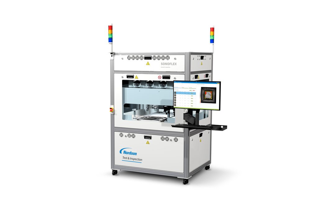
Nordson Test & Inspection will unveil its SonoFlex Acoustic Microscopy Inspection system, targeting inspection of semiconductor packages and small panels.
As semiconductor packaging becomes more complex, additional layers, materials, and interfaces can introduce defects that are difficult to identify through surface inspection. Voids, cracks, delamination, and other internal issues can affect package reliability even when the outside of the device appears intact.
SonoFlex uses acoustic imaging to examine these internal structures without requiring destructive analysis. This allows manufacturers to inspect packaged devices and identify potential defects while retaining the sample for further processing or analysis.
The system combines ThruScan imaging with new pulser and transducer technologies. According to Nordson, the combination can achieve scanning speeds up to twice those of conventional solutions while maintaining high-resolution imaging. This is intended to make acoustic inspection more suitable for production environments, where inspection speed needs to keep pace with manufacturing throughput.
SonoFlex also brings automated analysis into the inspection workflow. Its FlexCore software works with Nordson’s N-Intelligence Multi-Gate Image Analysis technology to identify defects and isolate voids within inspection data. This can reduce the amount of manual analysis required when examining complex devices and processes, particularly where large volumes of inspection data need to be reviewed.
The platform uses a modular architecture that allows multiple SonoFlex systems to be configured together as inspection requirements grow. Nordson says such configurations can increase overall throughput by up to eight times, depending on the system arrangement.
The technology is aimed at back-end semiconductor manufacturing, where non-destructive inspection can provide visibility into internal package structures and material interfaces. Rather than replacing other inspection techniques, acoustic microscopy can complement them by revealing defects that may remain hidden from surface-level inspection.