

Researchers have demonstrated a 0.34 × 0.34 nm² graphene-edge memristor that enables probabilistic-bit computing at 370 nW.
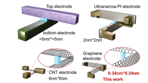
Researchers at Tsinghua University, working with Fudan University, have demonstrated an angstrom-scale graphene-edge memristor for low-power probabilistic computing. The device has a geometrically defined crossed-electrode area of 0.34 × 0.34 nm², exhibits a switching ratio exceeding 10³ and shows volatile switching behaviour.
The device is built around graphene transferred onto vertical sidewalls, placing the edge of the two-dimensional material between crossed electrodes. The 0.34-nm dimension corresponds approximately to the thickness of a single graphene layer. Instead of defining the active region through conventional planar lithography, the researchers use the geometry of the graphene edge and the crossed-electrode structure to establish the nanoscale switching region.
A memristor is a two-terminal device whose electrical resistance depends on its previous state. In the demonstrated device, the switching behaviour occurs at the exposed graphene edge. The researchers report a switching ratio exceeding 1000 and volatile characteristics, meaning that the device does not retain its state indefinitely after the applied stimulus is removed.
Fabricating the structure required a stress-distribution-based graphene transfer technique. The researchers used this approach to transfer graphene intact onto smooth vertical sidewalls. Chemical mechanical polishing (CMP) was then used to planarise the structure, followed by wafer-level bonding to integrate the device. The authors identify the combination of these techniques as an approach for constructing graphene-edge devices with geometrically defined nanoscale electrode structures.
The reported power figure is one of the main results of the work. The researchers demonstrated low-power operation at 370-nW while using the device in a probabilistic-bit system. The paper does not present this simply as the power consumption of a conventional memory write; rather, the 370-nW result comes from the demonstrated probabilistic-computing application.
Probabilistic bits, or p-bits, are computing elements whose states fluctuate between values according to a probability distribution. Unlike conventional digital bits that are designed to remain in a defined 0 or 1 state, p-bits can be used in probabilistic computing architectures for tasks such as optimisation and sampling. The stochastic switching behaviour of the graphene memristor provides a physical mechanism for generating this probabilistic behaviour.
This makes the volatile nature of the device useful rather than a limitation for the demonstrated application. A volatile memristor is not suitable as a direct replacement for non-volatile memory where data must remain stored after power is removed. For probabilistic computing, however, controlled state fluctuations can provide the randomness required by p-bit architectures.
The researchers describe the device as an angstrom-scale memristor and demonstrate its potential for high-density arrays. The geometrically defined 0.34 × 0.34 nm² crossed-electrode area is particularly relevant to scaling because the active region is established by the graphene edge rather than by reducing a conventional planar device indefinitely. The paper also presents the fabrication approach as a way of manipulating two-dimensional materials in unconventional geometries.
The work remains a laboratory demonstration rather than a commercial memory technology. The researchers demonstrate individual devices and a probabilistic-bit system, but moving from such structures to large, manufacturable arrays would require further work on integration, uniformity, yield, reliability and process scalability. The paper’s emphasis is therefore on demonstrating the device concept and fabrication approach rather than presenting a production-ready memory platform.
For chip designers, the significance is less about replacing existing memory immediately and more about providing another physical route to probabilistic computing. Conventional CMOS systems can generate random behaviour using dedicated circuits, while emerging devices such as memristors can incorporate stochastic behaviour directly into the computing element. Such approaches could eventually be explored for optimisation, machine learning and other workloads that benefit from probabilistic processing.
The research also demonstrates how two-dimensional materials can be incorporated into device structures that are difficult to realise with conventional planar processing. The stress-engineered transfer, CMP, and wafer-bonding sequence provides a possible fabrication route for integrating graphene into vertical device geometries. The authors suggest that the approach could support future high-density memristor arrays.
For Indian semiconductor and electronics researchers, the immediate opportunity is likely to be in the architecture and algorithm side of probabilistic computing rather than manufacturing the demonstrated graphene device. Probabilistic algorithms and optimisation methods can be developed and evaluated using conventional processors and FPGA platforms while researchers investigate emerging device technologies for future hardware implementations.
The demonstrated 370-nW probabilistic-bit operation shows how an atomically thin material can be used not merely as a passive electronic layer but as the active element of a computing architecture. The next challenge is translating the nanoscale device demonstration into reproducible arrays and practical systems that can exploit its low-power probabilistic behaviour.
For more information, click here.