


The latest computing technology is an in-memory processor that improves AI and machine learning efficiency, revolutionizing data processing.
Researchers at the École Polytechnique Fédérale de Lausanne (EPFL) have developed the world’s most extensive in-memory processor using a two-dimensional semiconductor material. This innovation marks progress towards enhancing computational efficiency, especially for resource-intensive tasks in machine learning (ML) and artificial intelligence (AI), applicable to devices within the Internet of Things (IoT) network.

The design bottleneck, which prevents simultaneous data and instruction fetch operations, highlights an opportunity to enhance efficiency. This is precisely the area where in-memory computing becomes significant.
An in-memory processor works directly on stored data, eliminating the need to transfer it to and from a central processor. Current developments focus on integrating storage and processing into unified in-memory processors, which incorporate elements functioning as memory and transistors. The material used for this purpose is molybdenum disulfide (MoS₂), employed to construct a two-dimensional transistor. The initial prototype was created by extracting a MoS₂ layer from a crystal with Scotch tape.
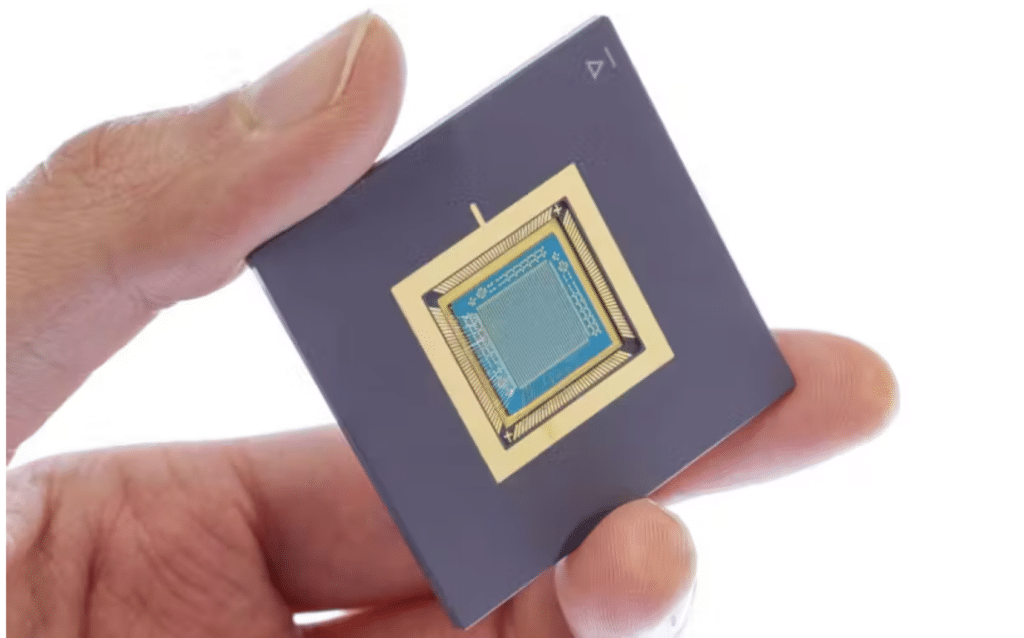
The researchers have created a large-scale chip to demonstrate this concept, integrating 1,024 transistors with floating gates that serve as memory and control the conductivity of the attached transistor. By adjusting each transistor’s conductivity, they can perform analogue vector-matrix multiplication in one step, applying voltages to the processor and measuring the output. This approach has been demonstrated for vector-matrix multiplication and signal-processing tasks.
The breakthrough in this project lies in the device’s scale, with its chip comprising 1,024 transistors to form a 32×32 vector-matrix multiplier, the largest of its kind. Building such a device is not as difficult as it might seem, mainly due to advancements in depositing high-quality material, which has been vital in scaling from a single transistor to over a thousand.
It is now possible to manufacture entire wafers coated with a uniform layer of MoS₂ after extensive process optimisation. This advancement enables the use of industry-standard tools for designing integrated circuits on computers and converting these designs into physical circuits, paving the way for mass production.
