


- Allows testing of up to 3000 die simultaneously from previous 1500 die testing
- Incorporates new custom electronics for enhanced signal integrity to enable highly parallel tests
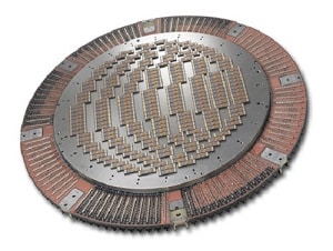 FormFactor, a semiconductor test and measurement supplier, has reached a high-throughput milestone in DRAM wafer testing with the release of the SmartMatrix 3000XP probe card. The new SmartMatrix 3000XP probe card allows DRAM manufacturers to test 3000 die or more at once using FormFactor’s proprietary Tester Resource Enhancement (ATRE) and MEMS probe technologies. The new breakthrough allows simultaneous test of approximately 1000 additional die over previous capabilities and can reduce the test cost per die by more than 25 per cent.
Increased die count
The DRAM industry’s migration to the 1Z and 1α nanometer process node from the previous 1X and 1Y nodes continues the trend to increased die count on wafer. As a result, full-wafer DRAM probe cards that simultaneously test every die on the wafer must keep pace. Built on a scalable DRAM probe-card architecture, the SmartMatrix 3000XP incorporates new custom electronics to enhance signal integrity while leveraging massive tester resource to enable highly parallel test at the 1Z and 1α nanometer nodes.
“The technology built into our advanced DRAM probe cards provides customers a way to keep test costs in check, increase throughput of a test cell and ramp to high volume production quickly,” said Matt Losey, Senior VP and GM of the Probes Business Unit at FormFactor. “The SmartMatrix probe card, with its scalable MEMS probe technology, helps accelerate our customers’ yield and performance knowledge while meeting their aggressive die shrink roadmap.”

The SmartMatrix 3000XP probe card’s key features include:
- Proprietary TTRE (Terminated Tester Resource Enhancement) technology, enabling parallel test of 3000 die for low test cost
• Ultra-high switch-density ATRE (Advanced Tester Resource Enhancement) components allowing efficient component placement on existing 520mm PCB tester platforms
• Industry-leading test temperature range, from -40 degrees Celsius to 125 degrees Celsius, with a single probe card design for optimal operational efficiency
• Proven low-force 3D MEMS probe technology, enabling more than 150,000 probes per card at 1Z and 1α tech nodes pitch requirements. The platform supports the next generation 3D MEMS probe technology for ultra-small DRAM die
• Test clock rates up to 200 MHz at wafer sort, significantly increasing throughput and test coverage without compromise on test times
The 1Z DRAM node will move to high volume production later this year.