


With the potential to dramatically improve color accuracy, resolution, and even enable hyperspectral imaging, this breakthrough could reshape everything from smartphone cameras to medical diagnostics.
Every smartphone and digital camera today uses image sensors—devices that detect light much like the human eye. Just as cone cells in our retina recognize red, green, and blue (RGB), pixels in image sensors absorb these light wavelengths and convert them into electrical signals. Most image sensors are made from silicon, a material that naturally captures the entire visible spectrum. To isolate individual colors, filters are applied to each pixel. Unfortunately, this design wastes two-thirds of the incoming light, as each pixel only captures one color.

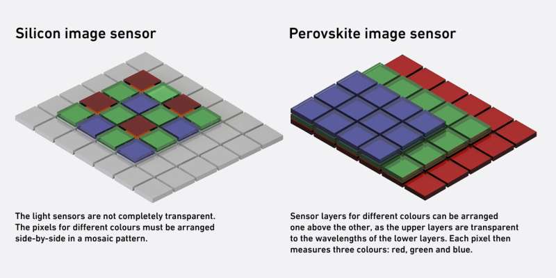
Researchers led by Maksym Kovalenko at ETH Zurich and Empa have developed a groundbreaking alternative: perovskite-based image sensors. Their research outlines how this new approach could triple the efficiency and resolution of traditional sensors. The key lies in a material called lead halide perovskite, a semiconductor that can be chemically adjusted to absorb specific colors. By slightly changing its composition—adding iodine for red, bromine for green, or chlorine for blue—researchers created layers that each capture a different color of light, without the need for filters. These layers are stacked vertically, unlike the horizontal layout of silicon pixels.
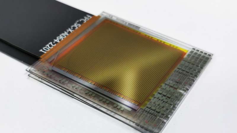
This stacking method allows all the light to be used, significantly boosting image quality and color accuracy. Two thin-film prototypes have already been built, proving the tech can be scaled down from lab-sized crystals to practical devices.Beyond photography, these sensors could power hyperspectral imaging, where multiple light wavelengths (beyond RGB) are analyzed.
This is crucial in fields like medical diagnostics, agriculture, and environmental monitoring. Perovskite sensors offer fine-tuned wavelength control without the bulky filters and heavy processing silicon systems require.While still in early development, the researchers aim to shrink pixel sizes from the current 0.5–1 mm to the micrometer scale, typical in commercial devices. This will require rethinking readout electronics designed for silicon.
