


A new method for creating 3D integrated circuit connections has now been developed. It works at low temperatures and does not require external pressure.
A new technique for the direct three-dimensional bonding of copper electrodes with silver was created by researchers from Osaka University’s Flexible 3D-System Integration Laboratory. This technique can lower the price and energy needs of new electronic products. The development of more energy-efficient and compact next-generation smart gadgets could benefit from the work done here.

Electronic devices are using three-dimensional integrated circuits more and more frequently. These topologies can conserve space and lessen the amount of material needed to connect the wires as compared to traditional 2D circuits. Contrary to the established technology used for conventional integrated circuits, reliable 3D connections require novel techniques. “Our process can be performed under gentle conditions, at relatively low temperatures and without added pressure, but the bonds were able to withstand over one thousand cycles of thermal shocking from -55 to 125 ºC,” first author Zheng Zhang says.
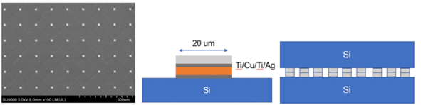
The two copper surfaces that will be joined using this novel technique are first sputtered with silver at room temperature. The silver layers were then heated to anneal them, which triggered “stress migration,” a microscopic alteration in the surface. A suitable effective area between the two silver layers was ensured by the surface roughening caused by the stress release during annealing. As a result, even at a relatively low annealing temperature, bonding may be done without the application of pressure. In ten minutes, permanent connections as small as 20 micrometres could be created. Additionally, this procedure only needs moderate temperatures (180 °C) and may operate in an atmosphere.
Using images from scanning electron microscopy and atomic force microscopy, the team was able to confirm the surface roughness of the sputtered and annealed chips. “This technology is expected to contribute to chips with a high density of interconnects and advanced 3D packaging,” senior author Katsuaki Suganuma says.
