


The use of 3D interconnects in miniaturized photonic power devices, results in a sixfold increase in wafer area utilization.
The University of Ottawa, collaborating with national and international partners, has successfully manufactured the world’s first back-contact micrometric photovoltaic cells. Remarkably small, these cells are only twice the thickness of a human hair. They offer considerable advantages over traditional solar technologies, primarily by reducing the shadowing caused by electrodes by 95%. This innovation has the potential to significantly lower the costs of energy production, potentially reducing them by up to three times.
To advance chip miniaturization and increase power density, a novel approach to fabricate 3D interconnects on multijunction solar cells has been developed. This process incorporates techniques like III-V heterostructure plasma etching, gold electro-deposition, and chemical-mechanical polishing, integrating through-substrate vias into the heterostructure.
Thin III-V films, as small as 20 micrometers, are managed through wafer bonding. This method has successfully produced photonic power devices that are smaller by three orders of magnitude, compared to standard chips, while maintaining a minimal shading factor below 3%.
The use of 3D interconnects, in contrast to traditional 2D connections in miniaturized photonic power devices, results in a six-fold increase in wafer area utilization. These advancements not only improve power yield per wafer but also pave the way for high-density, miniaturized devices in applications like power over fiber, the internet of things, and micro-concentrator photovoltaics.
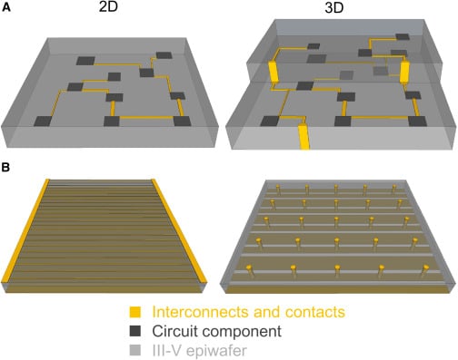
This study showcases a pioneering approach to enhancing power devices through three-dimensional (3D) interconnects, particularly focusing on III-V heterostructures. Traditionally, the challenge in power device densification has been navigating the limitations of two-dimensional lithography and packaging. 3D integration, already refined in silicon-based electronics, offers a viable solution to this challenge.
This work demonstrates the potential of 3D interconnects in various power devices, including GaN and SiC power-electronic modules, high-frequency devices like high electron mobility transistor (HEMTs) and hetero-junction bipolar transistors (HBTs), betavoltaic devices, and thermophotovoltaic converters. The key benefit of 3D interconnects in these applications is the reduction in shading, parasitic dark current, and resistive losses, thus increasing power density and efficiency.
