
A novel dielectric (insulator) component for transistors has been created by researchers at UNSW Sydney that is small, transparent, and flexible. Electronics made on traditional silicon semiconductors would be able to shrink without losing functionality thanks to the new material.
The researchers claim that this material is one of the most important barriers to overcome for the creation of a new generation of futuristic electronic gadgets, including augmented reality, flexible screens, novel wearables, and several uses that have not yet been discovered.

“Not only does it pave a critical pathway to overcome the fundamental limit of the current silicon semiconductor industry in miniaturization, but it also fills a gap in semiconductor applications due to silicon’s opaque and rigid nature,” says Professor Sean Li, UNSW Materials and Manufacturing Futures Institute (MMFI) Director and principal investigator on the research. “Simultaneously, the elastic and slim nature could enable the accomplishment of flexible and transparent 2D electronics.”
To create the transparent field-effect transistors for the study, MMFI engineers used a freestanding single-crystal strontium titanate (STO) membrane as the gate dielectric. They found that the performance of their new, smaller devices was comparable to that of modern silicon-semiconductor field-effect transistors.
“The key innovation of this work is that we transformed conventional 3D bulk materials into a quasi-2D form without degrading its properties,” says Dr. Jing-Kai Huang, the paper’s lead author. “This means it can be freely assembled, like LEGO blocks, with other materials to create high-performance transistors for a variety of emerging and undiscovered applications.”
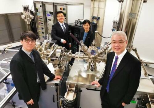
“Fabricating devices involves people from different fields. Through MMFI, we have established connections with academics who are experts in the 2D electric device fields as well as the semiconductor industry,” says Dr. Ji Zhang, a co-author of the paper.
“The first project was to fabricate the freestanding STO and to study its electrical properties. As the project progressed, it evolved into fabricating 2D transistors using freestanding STO. With the help from the platform established by MMFI, we were able to work together to finish the project.” Currently, the team is aiming for wafer-scale production. They want to test whether they can use the material to create all the circuits for a whole computer on a single chip.
Click here to read their study.