
These devices can significantly cut down on weight, footprint, and complexities.
Deep UV frequencies that would otherwise be absorbed by the Earth’s ozone layer are detected and classified by a variety of instruments and detectors. The bulk of solar-blind space-borne imaging systems still rely on photomultiplier tubes and/or microchannel plates with silicon photodiodes, adding to the devices’ complexity and weight.

After decades of development, Indian researchers are wondering why ultrawide bandgap (UWBG) photodetectors with deep UV capabilities have not seen broad acceptance. “From the device and materials point of view, enough advances have been made. Now, it is time to bring systems and imaging experts and device and materials engineers together to study and qualify UWBG detectors under actual conditions for real-world applications”, says Digbijoy Nath, Study Author, Centre For Nano Science and Engineering, Indian Institute of Science.
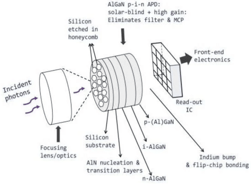
For industrial and biological purposes, as well as strategic and astronomical concerns, the ability to scan with UV is critical. UWBG photodetectors built on aluminium gallium nitride and gallium (III) oxide are more effective than silicon-based counterparts, allow for unique cutoff wavelengths, and do not require optical filters to filter out visible and infrared wavelengths for solar-blind applications.
Instead of the often used photo-to-dark current ratio, transient responses, responsivity, and other parameters, the researchers propose new criteria for evaluating photodetectors that consider gain, noise, and bandwidth.
In addition to determining how durable and dependable devices are in real-world applications, the researchers say more study is needed to improve how materials are built over large areas of substrates using an epitaxy approach that involves depositing crystals onto a thin film.
“It’s high time now for the community to have a pull from the industry and strategic sector so that device and material engineers can start working with imaging and systems groups to actually develop focal plane arrays and to integrate these with front-end electronics for real-life testing and applications”, says Nath.