


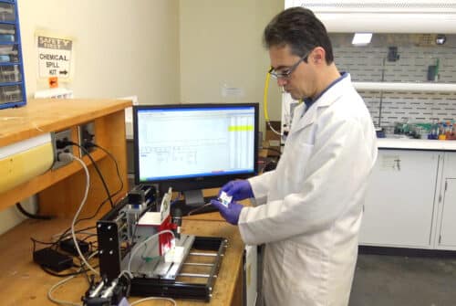
Wearable electronics are becoming more and more prevalent. Expanding on earlier research in this field that led to the approval of a patent this year Professor Arash Takshi and Professor Sylvia Thomas of USF (University of Southern Florida) Research & Innovation are using a cutting-edge electrochemical technique to print copper directly on fabric.
“The current technology for wearable electronics is mainly based on printing conductive inks consisting of nanoparticles of metals and/or carbon,” Takshi said. “The process relies on the physical connections of nanoparticles after drying the pattern. However, the high electric resistance from a conductive path made of conductive nanoparticles limits the applications to simple wearable electronic designs. These aren’t suitable for sensitive measurements and high electric current applications.”

More importantly, attaching electrical components to clothes is a difficult task since the fabrics might be harmed by the traditional soldering approach using a soldering iron, and conductive pastes are not robust enough for wearable electronics.
An additive manufacturing procedure in two steps is used in the novel fabrication technique. First, a conductive template is placed to materials via laser printing, which carbonises them. The circuit configuration is then created by electroplating copper to create a continuous copper design.
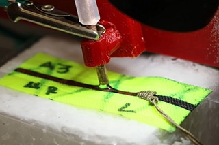
Localized electroplating is now possible thanks to the development of a nozzle installed on a platform for a 3-D printer. By using this technique, copper can be grown at the intersections of the terminals of electronic components and the printed layout of the circuit to solder them at room temperature. This new technique is similar to 3D printing if it were possible to create materials at the nanoscale.

The suggested procedure uses a few volts. The much greater voltage, which is still in the range of 2-3 V, and copper oxidation cause water electrolysis. This method, known as hydrogen evolution assisted (HEA) electroplating, pushes the copper’s growth constraints by achieving rates three orders of magnitude higher than standard electroplating. The mechanical stability of the printed structure is enhanced by the simultaneous electroplating and water electrolysis process, which also creates a growing copper structure in the form of a fern that seeps into the fabric strands.
Using this breakthrough technology, smart suits for astronauts and military personnel with distributed sensors can be created. Also, a patient’s health state and athletes’ physical activities can both be tracked using smart suits.
Click here to watch their demo on YouTube. Here are the patent details: A. Takshi, SM Rosa-Ortiz, Patent No. 11,214,884