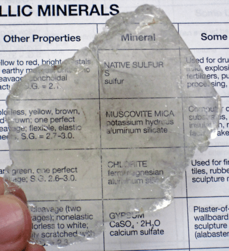
Many two-dimensional materials with distinct electrical and physical characteristics are being considered for the next generation of electronic devices. One such material is muscovite mica (MuM).

MuM has drawn interest as an ultra-flat substrate for creating flexible electrical devices, similar to how graphene has. However, MuM is an insulator, unlike graphene. It is composed of layers of silicon (Si), aluminium (Al), and potassium (K), but it’s electrical properties are unclear. Particularly, it is unclear how the characteristics of MuMs with single and few molecule layer thicknesses work. This is due to a quantum phenomenon known as “tunnelling.” Because of this, it has been challenging to comprehend the conductivity of thin MuM.
Professor Muralidhar Miryala from Shibaura Institute of Technology (SIT), Japan, Professors M. S. Ramachandra Rao, Ananth Krishnan, and Mr. Ankit Arora, a PhD student, from Indian Institute of Technology Madras, India, have recently observed a semiconducting behaviour in thin MuM flakes, characterised by an electrical conductivity that is 1000 times greater than that of thick MuM.
In order to prevent tunnelling, the researchers kept the contact electrodes apart by 1 m while exfoliating thin MuM flakes of different thickness onto silicon (SiO2/Si) substrates. When they measured the electrical conductivity, they discovered that as the flakes were reduced to fewer layers, the change to a conducting state happened gradually. They discovered that for MuM flakes smaller than 20 nm, the current varied with thickness, increasing by a factor of 1000 for a 10 nm thick MuM (5 layers thick), as opposed to a 20 nm thick MuM.
The “hopping conduction model” proposes that the observed conductance is caused by an increase in the conduction band carrier density with the reduction in thickness. Simply said, when MuM flakes become thinner, less energy is needed to transfer electrons from the solid bulk to the surface. This makes it simpler for electrons to enter the “conduction band,” where they may travel around freely and conduct electricity. The reason for the rise in carrier density was attributed by the researchers to the impacts of K+ ion-contributed surface doping (impurity addition) and MuM crystal structure relaxation.
This discovery is significant because it reveals that the band structure of thin exfoliated sheets of MuM is comparable to that of wide bandgap semiconductors. This makes thin MuM flakes a perfect material for two-dimensional electronic devices that are both flexible and robust, together with its exceptional chemical stability. “MuM is known for its exceptional stability in harsh environments such as those characterized by high temperatures, pressures, and electrical stress. The semiconductor-like behavior observed in our study indicates that MuM has the potential to pave the way for the development of robust electronics,” says Prof. Miryala.
Access their research here.


