Researchers have developed an all-optical pumping chip based nanolaser technology that can aid the ever-growing need to move more data faster.
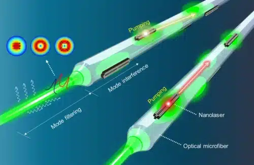
A new all-optical approach for driving multiple highly dense nanolaser arrays has been developed by researchers in Korea. This method can enable chip-based optical communication links that process and move data much faster than current electronic-based devices. Researchers have demonstrated that densely integrated nanolaser arrays — in which the lasers are just 18 microns apart — can be fully driven and programmed with light from a single optical fiber.

“Optical devices integrated onto a chip are a promising alternative to electronic integrated devices, which are struggling to keep up with today’s data processing demands,”research team leader Myung-Ki Kim from Korea University. “By eliminating the large and complex electrodes typically used to drive laser arrays, we reduced the overall dimensions of the laser array while also eliminating the heat generation and processing delays that come with electrode-based drivers.”
The new nanolasers could be used in optical integrated circuit systems, which detect, generate, transmit, and process information on a microchip via light. Instead of the fine copper wires used in electronic chips, optical circuits use optical waveguides, which allow much higher bandwidths while generating less heat. However, because the size of optical integrated circuits is quickly reaching into the nanometer regime, there is a need for new ways to drive and control their nano-sized light sources efficiently.
Researchers used electrodes with a unique optical driver that creates programmable patterns of light via interference. This pump light travels through an optical fiber onto which nanolasers are printed. To demonstrate this approach, the researchers used a high-resolution transfer-printing technique to fabricate multiple photonic crystal nanolasers spaced 18 microns apart. These arrays were applied onto the surface of a 2-micron-diameter optical microfiber. The interference pattern could also be modified by adjusting the driving beam’s polarization and pulse width.

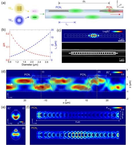
The experiments showed that the design allowed multiple nanolaser arrays to be driven using light traveling through a single fiber. The results matched well with numerical calculations and showed that the printed nanolaser arrays could be fully controlled by the pump beam interference patterns.
Reference : “Three-dimensional programming of nanolaser arrays through a single optical microfiber” by Myung-Ki Kim, Aran Yu, Da In Song, Polnop Samutpraphoot, Jungmin Lee, Moohyuk Kim, Byoung Jun Park, and Alp Sipahigil, 15 December 2022, Optica.
DOI: 10.1364/OPTICA.471715