


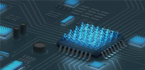
Researchers have discovered a blue form of ultrathin phosphorus with electronic properties that can enhance the injection of charge carriers into transistors.
Silicon, with its base in the world of technology, is not only the second most abundant element on earth’s crust but also the second most important element for our lives after oxygen. Silicon has proven its ability of being an ideal element to manipulate electricity in a very admirable way. Transition of ions can be barely achieved in any other element like silicon. But the current pace of transition can not be considered absolute.
A newly discovered blue form of ultrathin phosphorus—with electronic properties that can be tuned to enhance the injection of charge carriers (negatively and positively charged) into transistors—are set to push next-generation electronic devices forward.
A team of researchers led by Shubham Tyagi, a Ph.D. student, at King Abdullah University of Science and Technology has designed a junction-free FET using the recently discovered two-dimensional blue phosphorene as the single electroactive material. Blue phosphorene itself is a semiconductor but becomes a metal when stacked into a bilayer. “The ability of blue phosphorene to change its electronic properties based on stacking is crucial for our device,” Tyagi says. “Once we obtained a crystal orientation that delivers high carrier mobility through the channel, we were confident that we would achieve positive results because the contact resistance is addressed by the junction-free design,” he adds.
The blue phosphorene monolayer acts as the channel, at the heart of junction-free devices, lying between two metallic blue phosphorene bilayers that work as electrodes. The channel and electrodes consist of the same material, which results in a continuous structure, therefore reducing the resistance.

Researchers investigated the quantum transport in the proposed FET design for two different directions: armchair and zigzag using simulations. In both configurations, the FET effectively mediated electron transfer between channel and electrodes while meeting switching and amplification criteria. It outperformed devices using other two-dimensional materials, such as black phosphorene and monolayer molybdenum disulfide.
Researchers are working to reduce the current leakage between transistor gate and electrodes using van der Waals materials, which consist of sheets held together through weak interactions and expanding their ideas to develop spintronic devices.
Reference : Shubham Tyagi et al, High-performance junction-free field-effect transistor based on blue phosphorene, npj 2D Materials and Applications (2022). DOI: 10.1038/s41699-022-00361-1