


Researchers have developed a new process that will allow faster and more efficient spintronics devices that can be scaled down smaller than ever before.
The semiconductor industry is constantly trying to develop smaller and smaller chips that can maximize energy efficiency, computing speed, and data storage capacity in electronic devices. Spintronic devices, which leverage the spin of electrons rather than the electrical charge to store data, provide a promising and more efficient alternative to traditional transistor-based chips. These materials also have the potential to be non-volatile, meaning they require less power and can store memory and perform computing even after you remove their power source.

Researchers from University of Minnesota Twin Cities along with a team at the National Institute of Standards and Technology (NIST), have developed a breakthrough process for making spintronic devices that has the potential to become the new industry standard for semiconductors chips that make up computers, smartphones, and many other electronics.
Spintronic materials have been successfully integrated into semiconductor chips for more than a decade now, but the industry standard spintronic material, cobalt iron boron, has reached a limit in its scalability. Currently, engineers are unable to make devices smaller than 20 nanometers without losing their ability to store data.
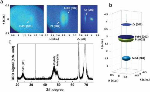
Researchers have shown that iron palladium, an alternative material to cobalt iron boron that requires less energy and has the potential for more data storage, can be scaled down to sizes as small as five nanometers. They were able to grow iron palladium on a silicon wafer using an 8-inch wafer-capable multi-chamber ultrahigh vacuum sputtering system, a one-of-a-kind piece of equipment among academic institutions across the country and only available at the University of Minnesota.
Deyuan Lyu, first author on the paper and a Ph.D. student in the University of Minnesota Department of Electrical and Computer Engineering says, “this work is showing for the first time in the world that you can grow this material, which can be scaled down to smaller than five nanometers, on top of a semiconductor industry-compatible substrate, so-called CMOS+X strategies.”
Reference : Deyuan Lyu et al, Sputtered L10‐FePd and its Synthetic Antiferromagnet on Si/SiO2 Wafers for Scalable Spintronics, Advanced Functional Materials (2023). DOI: 10.1002/adfm.202214201