


With over 75% transparency maintained, these sulfur-doped CuI films do not compromise the transparency for electronic applications.
Researchers at the University of Twente have made strides in advancing the conductivity of CuI by introducing sulfur (S) dopants through a method called pulsed laser deposition.

Copper iodide (CuI) has been recognized as the most effective p-type transparent conductor (TC) for some time, although its conductivity is not as high as that of n-type TCs. Detailed assessments combining both the composition and optoelectronic properties of the films revealed major conductivity improvements.
Incorporating 3% atomic sulfur into CuI significantly raises the hole carrier density from approximately 8 × 10^19 to 9 × 10^20 carriers per cubic centimeter. This increase elevates the conductivity from 78 to 435 Siemens per centimeter, while still retaining over 75% transparency in the visible spectrum.
The added sulfur promotes the creation of copper vacancies, which are essentially places where a copper atom is missing in the lattice structure of CuI. These vacancies increase the number of holes (positive charge carriers) in the material, which in turn boosts its electrical conductivity.

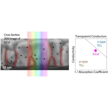
Sulfur’s presence is also seen in the grain boundaries (the interfaces between the crystalline structures within the material). Here, sulfur helps to create a mix of phases, likely including a CuxS phase, which has different electronic properties that contribute to the overall conductivity of the material.
This kind of material could be revolutionary for integrating electronic functionality into windows, screens, and potentially other transparent surfaces, without obscuring the view or altering the design.
The implications of such materials extend to various fields, from architectural design that integrates energy-generating solar panels into transparent surfaces to consumer electronics that could benefit from invisible circuits. This advancement in material science is a key step toward making such futuristic applications a practical reality.
