


The development of this n-channel diamond MOSFET marks a significant milestone in the quest for high-performance, resilient electronic devices.
The National Institute for Materials Science (NIMS) has made a groundbreaking contribution to electronics. Their researchers have successfully developed the first n-channel diamond MOSFET (metal-oxide-semiconductor field-effect transistor). This significant advancement opens up new possibilities for creating CMOS (complementary metal-oxide-semiconductor) integrated circuits designed for extreme conditions and the further evolution of diamond-based power electronics. Diamond semiconductors are recognised for their exceptional properties, such as a wide bandgap energy of 5.5 eV, high carrier mobilities, and superior thermal conductivity. These characteristics make them ideal for applications in harsh environments, like high temperatures and radiation levels, where traditional semiconductors fall short.

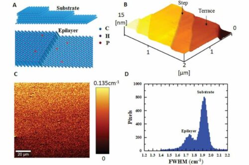
Diamond electronics offer better thermal management and excel in energy efficiency, withstanding higher breakdown voltages and more severe conditions. As the technology for diamond growth advances, the demand for diamond CMOS devices is on the rise to enable monolithic integration in power electronics, spintronics, and MEMS (microelectromechanical system) sensors that operate under extreme conditions. The fabrication of CMOS integrated circuits typically requires both p- and n-type channel MOSFETs, posing a significant challenge. The research team’s work in developing an n-channel diamond MOSFET is a substantial step toward addressing this challenge. The research team made a breakthrough by developing a method to grow high-quality monocrystalline n-type diamond semiconductors with atomic-level smoothness and flatness, achieved by doping diamonds with a low phosphorus concentration.
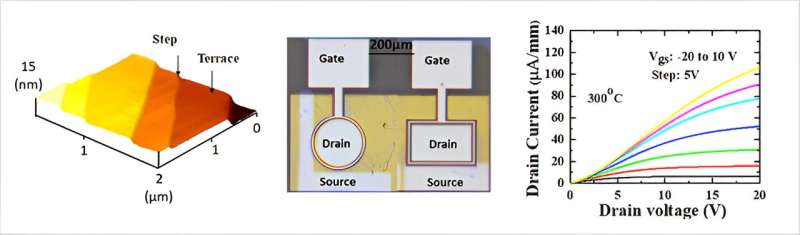
Using this technique, they successfully fabricated an n-channel diamond MOSFET, consisting of an n-channel diamond semiconductor layer on top of another diamond layer doped with a high phosphorus concentration. This structure significantly reduces the source and drain contact resistance, enabling the MOSFET to function effectively as an n-channel transistor. The team demonstrated the MOSFET’s high-temperature performance, with field-effect mobility—an important indicator of transistor performance—of approximately 150 cm2/V·sec at 300°C. This achievement is expected to accelerate the development of CMOS integrated circuits for energy-efficient power electronics, spintronic devices, and MEMS sensors that can operate in harsh environments.