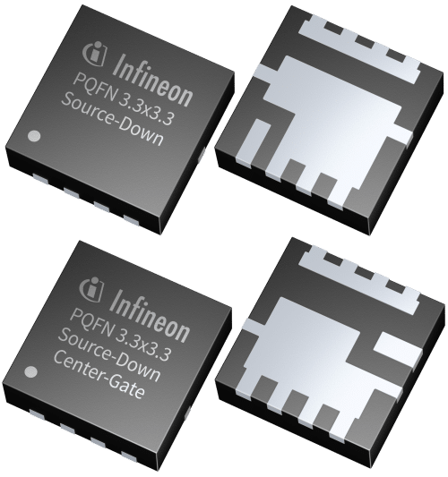
High power density, optimised performance, and ease of use are key requirements when designing modern power systems. To offer practical solutions for design challenges in end applications, Infineon Technologies AG launches the new generation of OptiMOS Source-Down (SD) power MOSFETs. They come in a PQFN 3.3 x 3.3mm2 package and a wide voltage class ranging from 25 V up to 100 V. This package sets a new standard in power MOSFET performance, offering higher efficiency, higher power density, superior thermal management and low bill-of-material (BOM). The PQFN addresses applications including motor drives, SMPS for server and telecom and OR-ing, as well as battery management systems.

Compared to the standard Drain-Down concept, the latest Source-Down package technology enables a larger silicon die in the same package outline. In addition, the losses contributed by the package, limiting the overall performance of the device, can be reduced. This enables a reduction in RDS(on) by up to 30 percent compared to the state of the art Drain-Down package. The benefit at the system level is a shrink in the form factor with the possibility to move from a SuperSO8 5 x 6 mm2 footprint to a PQFN 3.3 x 3.3 mm2 package with a space reduction of about 65 percent. This allows for the available space to be used more effectively, enhancing the power density and system efficiency in the end system.
Additionally, in the Source-Down concept, the heat is dissipated directly into the PCB through a thermal pad instead of over the bond wire or the copper clip. This improves the thermal resistance RthJC by more than 20 percent, from 1.8 K/W down to 1.4 K/W, thus enabling simplified thermal management. Infineon offers two different footprint
versions and layout options: the SD Standard-Gate and the SD Center-Gate. The Standard-Gate layout simplifies the drop-in replacement of Drain-Down packages, while the Center-Gate layout enables optimised and easier parallelisation. These two options can bring optimal device arrangement in the PCB, optimised PCB parasitics, and ease of use.


