
Littelfuse p-channel power MOSFETs, although less renowned than their widely used n-channel counterparts, have traditionally served a limited range of applications. However, with the increasing demand for low-voltage (LV) applications, the scope of p-channel power MOSFETs have been expanded. The simplicity of applying Littelfuse p-channel solutions for high-side (HS) applications makes them more attractive for LV inverters (< 120 V) and non-isolated point-of-load solutions. The ease of driving a HS p-channel MOSFET without the need for charge pump or additional voltage source results in simplified design, space savings, reduced part count and cost-efficiency. This article makes a basic comparison of n-channel and p-channel power MOSFETs, introduces Littelfuse’s p-channel power MOSFETs, and then explores their target applications.
A comparative analysis of n-channel and p-channel power MOSFETs
The cross-sectional view of the power MOSFET in Fig. 1 illustrates the differences between n-channel and p-channel power MOSFETs. While an n-channel MOSFET requires a positive gate-source voltage to activate, a p-channel MOSFET needs a negative gate-source voltage. The key distinction lies in their reverse doping profiles: p-channel MOSFETs rely on holes as the majority charge carriers, generating hole current, while n-channel devices utilize electrons, creating electron current. Due to electrons’ superior mobility, which is roughly 2 to 3 times that of holes, moving holes in a p-channel device is more challenging than electrons in an n-channel device. This leads to higher area-specific on-state resistance in p-channel MOSFETs compared to n-channel MOSFETs. Consequently, achieving equivalent on-state resistance (RDS(on)) performance is impractical for p-channel MOSFETs of the same chip size as n-channel MOSFETs.

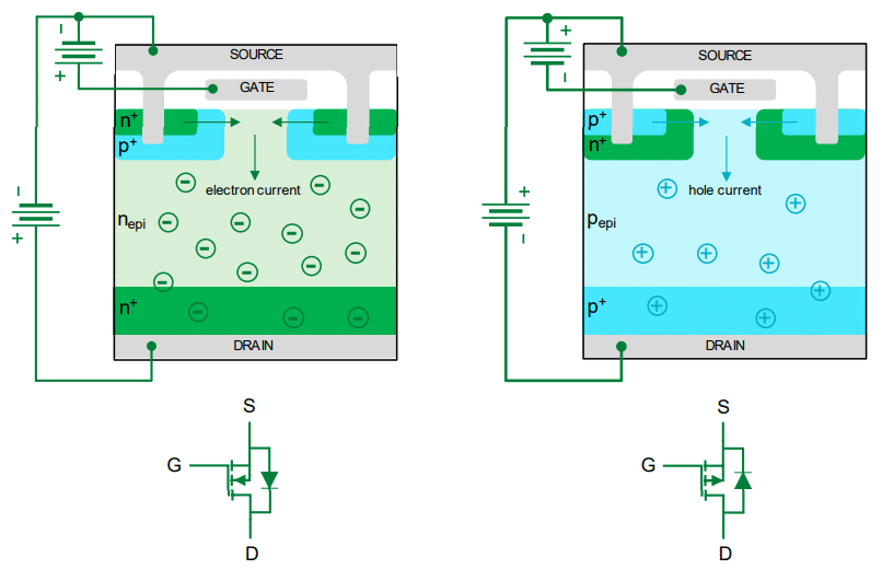
Fig. 1: Cross sections of an n- and p-channel power MOSFETs with their symbols
To achieve the same on-state resistance RDS(on) as the n-channel type MOSFET, the p-channel requires a 2 to 3 times larger die size. Therefore, in high-current applications, where low conduction losses are crucial, large die p-channel MOSFETs with very low RDS(on) are suboptimal. While the larger chip size of the p-channel device offers improved thermal performance, it exhibits larger intrinsic capacitances and thus higher switching losses. This drawback significantly affects overall system cost, efficiency, and thermal management when the system operates at a high switching frequency.
In low-frequency applications with significant conduction losses, a p-channel MOSFET should match the RDS(on) of an n-channel MOSFET, requiring a larger chip area. Conversely, in high-frequency applications prioritizing switching losses, a p-channel MOSFET should align with the total gate charges of an n-channel counterpart, often having a similar chip size but a lower current rating. Therefore, choosing the right p-channel MOSFET demands careful consideration of device RDS(on) and gate charge (Qg) specifications along with the thermal performance.
Littelfuse p-channel power MOSFETs
Littelfuse offers a range of industrial qualified p-channel power MOSFETs with the highest voltage class, lowest RDS(on) and Qg, high avalanche energy rating, excellent switching performance and superior safe operating area (SOA) with best-in-class performance in both standard industrial and unique isolated packages. Littelfuse p-channel power MOSFETs retain the essential features of comparable n-channel power MOSFETs such as fast switching, efficient gate-voltage control, and excellent temperature stability.
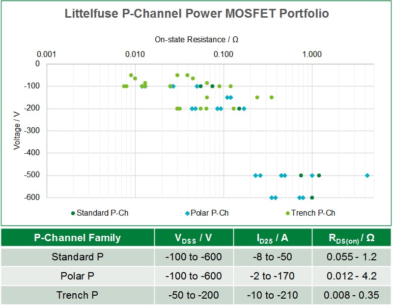
Fig. 2: Littelfuse p-channel power MOSFET portfolio
Fig. 2 presents the key highlights of p-channel power MOSFETs offered by Littelfuse. Standard P and PolarP™ planar devices are available with voltage ratings from -100 V to -600 V and current ratings from -2 A to -170 A. PolarP™ offers optimized cell structure with low area-specific on-state resistance and improved switching performance, while Standard P benefits from a better SOA performance. Trench P utilizing a more dense trench gate cell structure offers very low RDS(on), low gate charge, fast body diode and faster switching with device voltages ranging from -50 V to -200 V and currents from -10 A to -210 A. The latest addition to the portfolio is IXTY2P50PA (-500 V, -2 A, 4.2 Ω) which is Littelfuse’s first automotive grade p-channel power MOSFET for automotive applications.
Applications for Littelfuse p-channel power MOSFETs
Littelfuse p-channel power MOSFETs have a wide range of industrial and automotive applications like battery and reverse polarity protection, HS load switches, DC-DC converters, on-board chargers, and LV inverters.
P-Channel MOSFETs in half-bridge applications
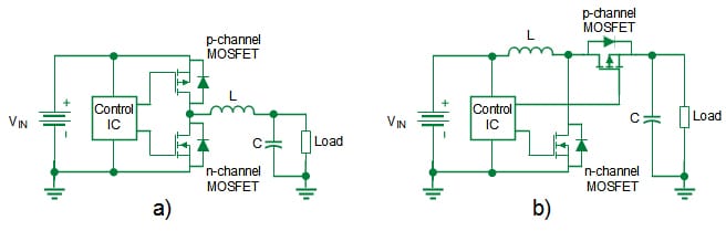
N-channel MOSFETs are typically used in the power stage in typical half-bridge (HB) applications. However, n-channel HS switches necessitate a bootstrap circuit to generate a gate voltage that is floating with reference to the source of the HS MOSFET or an isolated power supply to turn on as shown in Fig. 3a). Hence, the advantage of using n-channel devices comes at the cost of increased complexity in gate driver design leading to more design effort and greater space usage. Fig. 3 illustrates the contrast between circuits using complementary MOSFETs and those using n-channel MOSFETs. When a p-channel MOSFET is used as the HS switch in this configuration as depicted in Fig. 3b), it can greatly simplify the driver design. A charge pump that drives the HS switch could be removed and the p-channel MOSFET can be easily controlled by the MCU through a simple level shifter. This reduces design effort and part number count resulting in a cost-efficient design that utilizes space efficiently.
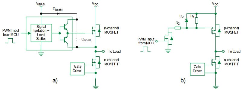
Fig. 3: Simplification of the HS driver in HB application from a) n-channel MOSFET to b) p-channel MOSFET as HS switch
Reverse polarity protection
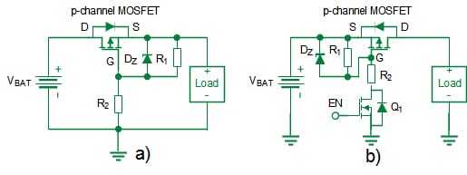
Reverse polarity protection is a safety measure within systems to prevent potential fire hazards and damages caused by a reverse connection of the power source. Fig. 4a) shows the reverse polarity protection implemented using a p-channel power MOSFET. When the battery is correctly connected, the intrinsic body diode conducts until the MOSFET channel is activated. In the event of a reverse connection of the battery, the body diode is reverse-biased, with the gate and source at the same potential, thereby turning off the p-channel MOSFET. A Zener diode clamps the gate voltage of the p-channel MOSFET, protecting it in case of excessively high voltage levels.
Load switch
Load switches connect or disconnect a voltage rail to a specific load offering a cost-effective and a simple way for a system to efficiently manage power. Fig. 4b) demonstrates a circuit using a p-channel power MOSFET for a load switch. This circuit is driven by a logic enable (EN) signal controlling the p-channel load switch via a small-signal n-channel MOSFET Q1. When EN is low, Q1 is off, and the p-channel gate is pulled up to VBAT. Conversely, when EN is high, Q1 activates, grounding the p-channel gate, turning on the load switch. If VBAT exceeds the p-channel MOSFET’s threshold voltage, it can turn on when EN is high, eliminating the need for an additional voltage source to bias the gate, which is necessary for n-channel MOSFETs. The series resistor is needed to limit the current and a Zener Diode to clamp the gate voltage to a maximum value.
DC-DC converters
In low-power DC-DC converters like the synchronous buck converter in Fig. 5a), using a p-channel device as the HS switch simplifies the circuit and saves space, eliminating the need for external gate driving circuitry. It also reduces the bill-of-materials (BOM), leading to cost efficiency. Similarly, in synchronous boost converters, a p-channel device can replace a diode with low forward voltage as an output synchronous rectifier, as seen in Fig. 5b). This improves the converter efficiency due to the improved figure-of-merit (FoM = RDS(on) * Qg) of the p-channel MOSFET
Conclusion
With the development of modern LV applications, Littelfuse’s p-channel power MOSFETs prove their versatility in meeting the evolving needs of today’s power electronics. Employing Littelfuse’s comprehensive range of p-channel MOSFETs provides designers with advantages such as simplified, more reliable, and optimized circuit design in industrial and automotive applications. To achieve optimal performance for specific applications, designers must assess the trade-off between RDS(on) and Qg when selecting a p-channel power MOSFET.
Author: Sachin Shridhar Paradkar, Product Marketing Engineer, Si & SiC discrete MOSFET, Littelfuse Europe GmbH
Sachin Shridhar Paradkar is the Product Marketing Engineer for Littelfuse Si & SiC discrete MOSFET devices. He previously served as a power electronics development engineer for motor drives and joined Littelfuse in June 2022. His current role entails fostering cross-functional collaboration to build and sustain product lines, discerning market needs, defining product roadmaps and requirements for new development, developing marketing collateral to promote existing portfolio and new product launches while staying updated on market trends and competition activity. Sachin earned his BS in Electrical & Electronics Engineering from Visvesvaraya Technological University (VTU), India and his MS in Electrical Power Engineering from RWTH Aachen, Germany.