


The mobility ecosystem continually introduces new issues for automotive design, particularly with regard to the size, safety, and reliability of electronic solutions. Then, new solutions are developed to address the technology challenges, adding connectivity and cloud computing through Electronic Control Units (ECUs).
High-end vehicles use up to hundreds of ECUs and this requires more efficient power management with safer power paths from the car battery to the load points to reduce failures. Electric safety can be enhanced by replacing conventional fuses, based on the principle that a conductor overheats and melts during an overload condition, with Electronic Fuses (eFuses). They are able to clamp the output voltage and limits the throughput current, appropriately supplying the load or eventually disconnecting it in the event of a persistent fault. High current environments impose strict constraints in terms of handling high-energy discharges, so robust and reliable power switches are needed.
High-Current Power Switch
The high-current power switch is a low resistance MOSFET connected in series to the main power rail and controlled by logic circuitry, which integrates various protection, diagnostic and monitoring features. In high power automotive systems, a bidirectional control is guaranteed through MOSFETs in a back-to-back configuration, which offers robust power path protection (Fig. 1).
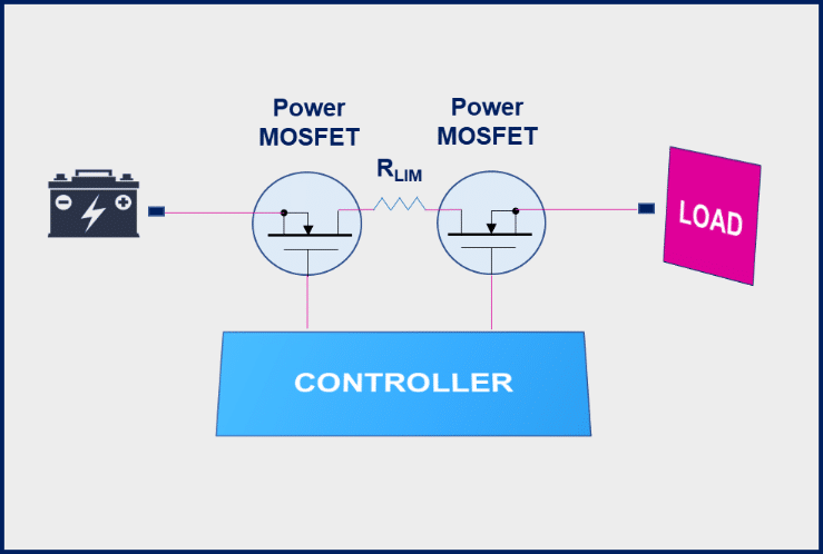
The current flowing in the power rail is detected in real time through the resistor (RLIM) and kept constant by the eFuse, which tunes the gate-source voltage (VGS) of the MOSFETs to limit the current to the target value. If a strong overcurrent or short circuit occurs, the controller disconnects the load, thus protecting the power supply.
At start-up, the eFuse provides a defined ramp-up of the output voltage to ensure the inrush current is maintained within safe confines, thus protecting both the load and the power supply. This condition places a severe constraint on the power MOSFETs which have to manage the soft charge phase of the bulk capacitor array present at the ECU input, withstanding a constant current under linear mode operation.
Furthermore, when the load is disconnected, the power MOSFETs are put into a stressed condition due to the discharge of the energy stored in the parasitic stray inductance associated to the wire harness which connects the main battery to the load of the final application.
In conclusion, the power MOSFETs have to meet the following requirements (Tab. 1):
| Power MOSFET | |
| Working Condition | Requirement |
| On-state | Low conduction loss |
| Start-up | Linear mode ruggedness |
| Turn-off | Energy handling |
The new STPOWER STripFET F8 MOSFET technology released by STMicroelectronics and fully AEC Q101 qualified exhibits all the key design improvements which ensure a high level of power efficiency and ruggedness for safe and reliable performance.
The STL325N4LF8AG is a 40V MOSFET housed in a PowerFLAT 5×6 leadless package with a sub-milliohm static on-resistance (RDS(on)), which is less than 0.75mΩ. Therefore, it is capable of providing very limited conduction losses.
Key Parameters for MOSFET Selection
For conventional automotive loads powered by the 12V lead-acid battery, the power switch has to withstand a continuous current flow up to 160 A – 200 A requested by the ECU for a power delivery in the range of 1kW.
1. Start-up Condition
In addition to the high current, the power MOSFET has to manage the pre-charge phase of the bulk capacitor array present at the input of the ECU to ensure a soft ignition. This requires a constant current for producing a smooth voltage rise at the ECU’s input pins, thus avoiding any high voltage ringing and current spikes.
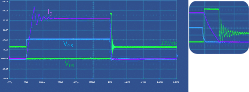
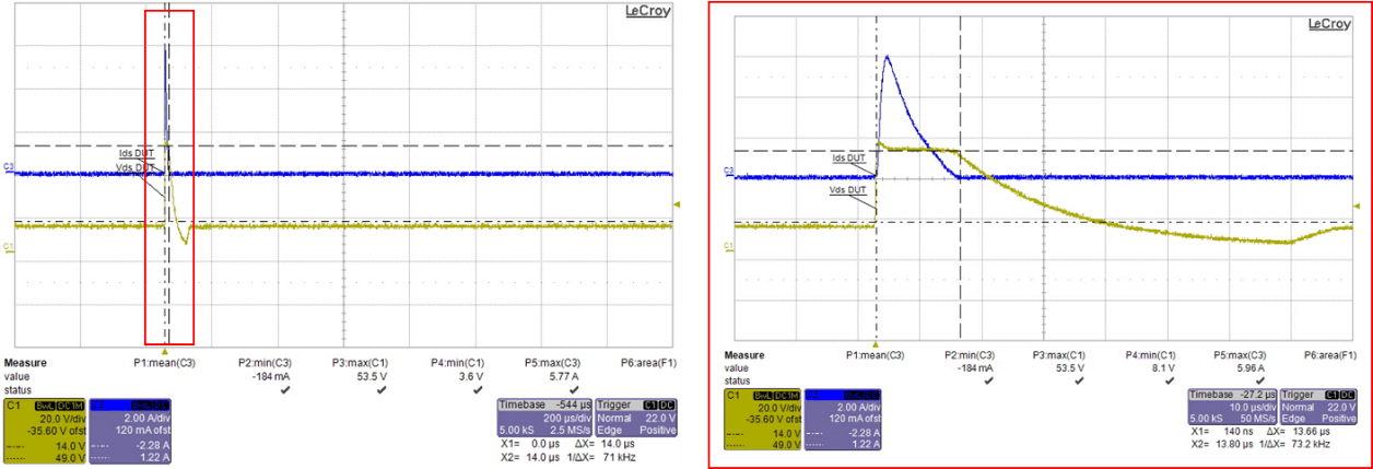
The ruggedness during the soft charge phase can be benchmarked with the circuit schematic shown in Fig. 2.
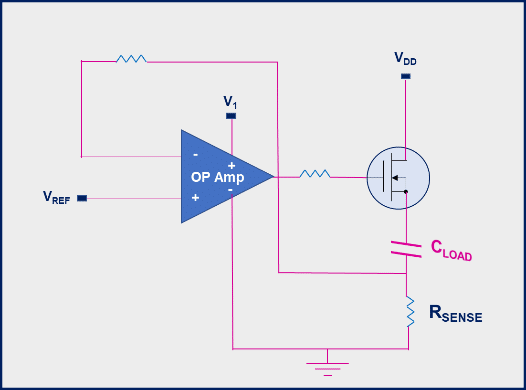
The circuit allows to charge the load capacitance (CLOAD) with constant current: by tuning the V1 and VDD voltage values, the current can be kept constant, thereby setting a specific charging time for CLOAD. The test was carried out with a 94mF stack of capacitors for the load and supply voltage of 15V.
For the STL325N4LF8AG, two different measurement settings are considered:
- case 1 – one device with a current of 1.7A for 700ms;
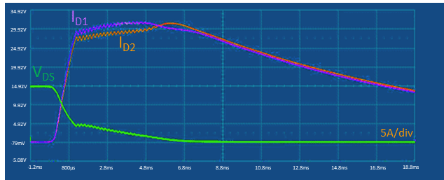
- case 2 – two devices in parallel with a current of 29A each for 6ms.
The measured waveforms for the linear mode operation are shown in Figs. 3 (for case 1) and 4 (for case 2)
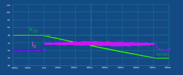
In case 1, the linear mode ruggedness of the power switch is tested for a long pulse time, which is close to DC operation.
In case 2, the two devices connected in parallel have the following gate threshold voltage (Vth) values:
- Vth1 = 1.49V @ 250µA
- th2 = 1.53V @ 250µA.
The limited Vth spread (in the 3% range) produces a tight imbalance on the MOSFET currents as follows:
- ID1 = 29A
- ID2 = 28.5A
where ID1 is slightly higher than ID2 for the lower Vth value.
In this case (2), the linear mode ruggedness of the power switches is tested at high current with a pulse time lasting a few milliseconds.
In both cases, the power MOSFET is capable of withstanding the linear mode working conditions, which match the theoretical safe operating area (SOA), preventing the device from any thermal runaway.
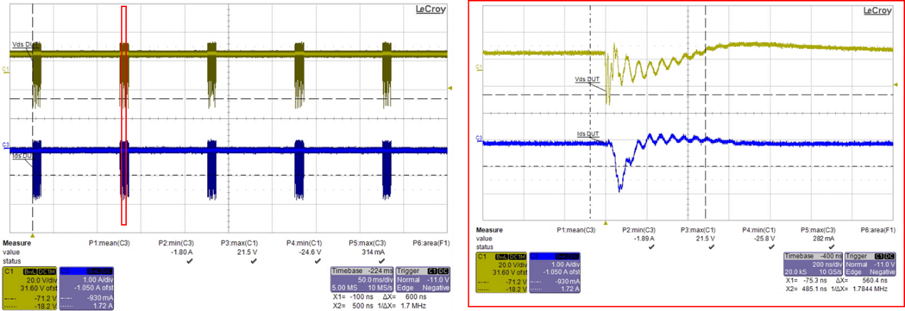
1. Turn-off Condition
The power MOSFET has to withstand a huge energy discharge stress at turn off. In fact, the wire harness connecting the main battery to the final application control board results in a high impedance associated to the parasitic stray inductance and this causes a huge energy discharge on the power distribution systems.
This energy can be managed with a single avalanche event at MOSFET turn-off in case of specific issues for the ECU or an active clamp which forces the MOSFET to work in linear mode again. The STL325N4LF8AG can properly work in a specific avalanche test at 40A, as shown in Fig. 5:
The device also has a rugged performance at turn-off in terms of energy management.
Compliance to ISO 7637-2
For 12V/24V battery systems, automotive eFuse switches have to fulfill the major obligations imposed by the international ISO 7637-2 standard, which is related to the transients generated on the supply rail. They can range from severe low to high energy or high to low energy level, in some cases with high dv/dt.
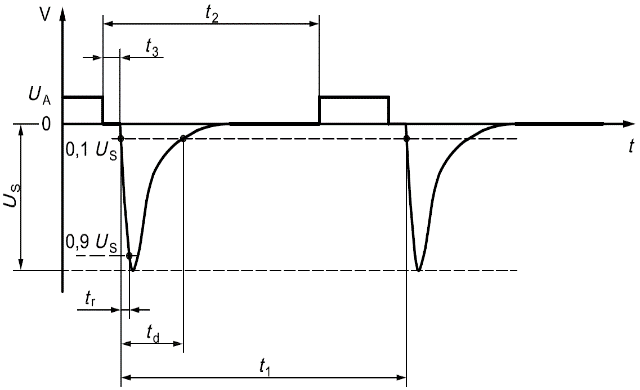
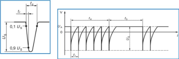
1. ISO 7637-2 Pulse 1
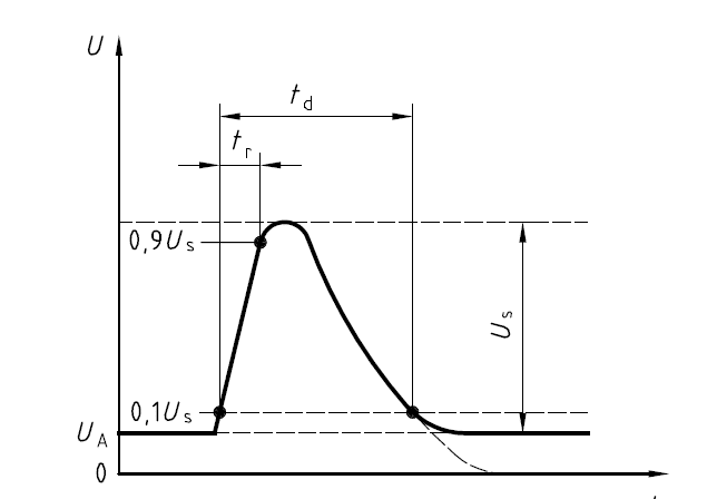
Pulse 1 describes the negative transient observed by electronics connected in parallel with an inductive load when the connection to the power supply is interrupted, as shown in Fig. 6.
| Parameter | Value | Unit |
| UA | 13.5 | V |
| US | -100 | V |
| td | 2 | ms |
| tr | 1 (+0/-0.5) | µs |
| t1 | ≥ 0.5 | s |
| t2 | 200 | ms |
| t3 | < 100 | µs |
| Ri | 10 | Ω |
| Duration | 5000 | pulses |
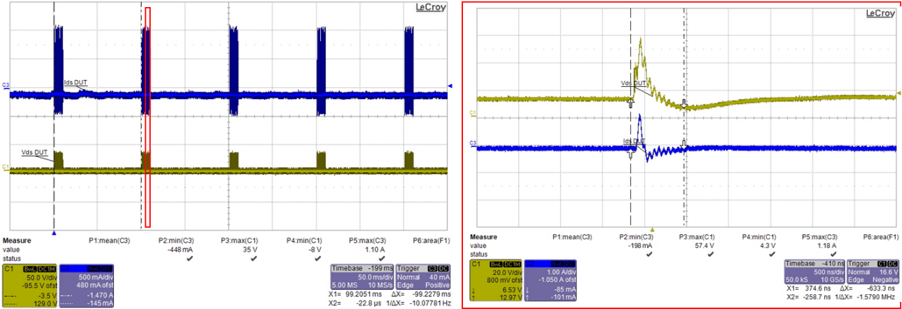
The compliance to ISO 7637-2 pulse 1 was verified for STL325N4LF8AG and the measurement results are shown in Fig. 7:
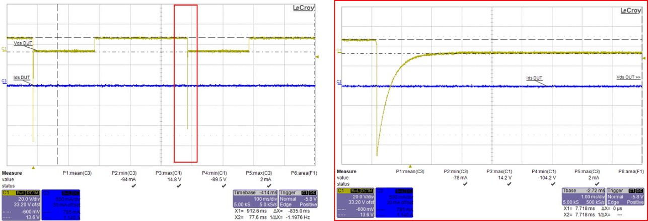
(zoomed on the right).
The experimental data show that STL325N4LF8AG can pass the ISO 7637-2 pulse 1 test without showing any failure or derating of the main parameters.
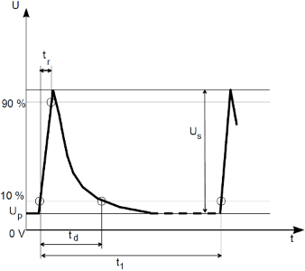
2. ISO 7637-2 Pulse 2a
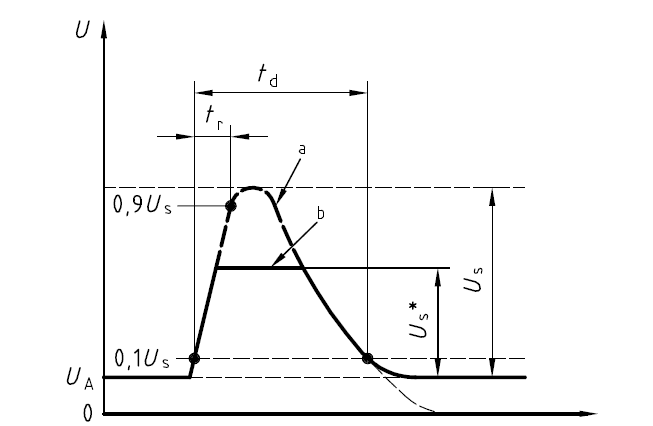
Pulse 2a describes the positive voltage spike that may occur when current is interrupted to a circuit in parallel with the electronics being tested, as shown in Fig. 8:
| Parameter | Value | Unit |
| UP | 13.5 ± 5% | V |
| US | +100 ± 5% | V |
| td | 50 ± 10% | µs |
| tr | 1 ± 10% | µs |
| t1 | 0.5 ± 10% | s |
| Ri | 10 ± 10% | Ω |
| Duration | 1 ± 10% | h |
The measurement results for STL325N4LF8AG for ISO 7637-2 pulse 2a are shown in Fig.9:
(zoomed on the right).
The STL325N4LF8AG can pass the test also in this case without showing any failure or derating of the main parameters.
3. ISO 7637-2 Pulses 3a and 3b
Pulses 3a and 3b define the negative spikes that may occur as a result of switching processes, influenced by the distributed capacitance and inductance of the wiring harness, as shown in Figs. 10 and 11:
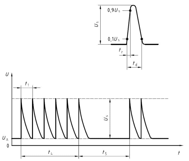
The parameters value for the tests are reported in Tab. 2:
| Parameter | Pulse 3a Value | Pulse 3b Value | Unit |
| UP | 13.5 | 3.5 ± 0.5 | V |
| US | -150 | +100 ± 5 % | V |
| td | 100 | 50 ± 45 | ns |
| tr | 5 | 5 ± 1.5 | ns |
| t1 | 100 | 100 ± 20 % | µs |
| t4 | 10 | 10 ± 20 % | ms |
| t5 | 90 | 90 ± 20 % | ms |
| Ri | 50 | 50 ± 20 % | Ω |
| Duration | 1 | h |
Experimental data for STL325N4LF8AG relevant to ISO 7637-2 pulse 3a and pulse 3b are shown in Figs. 12 and 13:
(zoomed on the right).
(zoomed on the right).
The test results are positive for STL325N4LF8AG for both pulse 3a and 3b too.
4. ISO 7637-2 Pulses 5a and 5b (Load Dump)
Pulses 5a and 5b are a simulation of load dump transient, occurring in the event of a discharged battery being disconnected while the alternator is generating charging current and with other loads remaining on the alternator circuit, as shown in Figs. 14 and 15:
The parameters value for the tests in a 12V system are reported in Tab. 3
| Parameter | Pulse 5a Value | Pulse 5b Value | Unit |
| US | 65 to 87 | 65 to 87 | V |
| US* | 35.2 | V | |
| td | 40 to 400 | 40 to 400 | ms |
| tr | 5 to 10 | 5 to 10 | ms |
| Ri | 0.5 to 4 | 0.5 to 4 | Ω |
The measured waveforms of STL325N4LF8AG with ISO 7637-2 pulse 3a and pulse 3b are shown in Figs. 17 and 18:

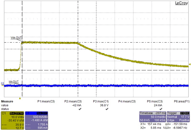
Then, the STL325N4LF8AG can provide a protection to load dump too.
Conclusions
The STL325N4LF8AG manufactured with the new STripFET F8 technology is tailored for withstanding all the stressful conditions associated to eFuse applications. The device is able to withstand the stressful working conditions at start-up and turn-off. Furthermore, the MOSFET successfully passes all the tests defined by the international standard ISO 7637-2 for conducted transients in 12V/24V battery systems. This best-in-class behavior makes the STL325N4LF8AG the ideal choice for safer power distribution systems in harsh automotive applications.
References
[1] R. Bojoi, F. Fusillo, A. Raciti, S. Musumeci, F. Scrimizzi and S. Rizzo, “Full-bridge DC-DC power converter for telecom applications with advanced trench gate MOSFETs”, IEEE International Telecommunications Energy Conference (INTELEC), Turin 2018.
[2] S. Musumeci, F. Scrimizzi, G. Longo, C. Mistretta and D. Cavallaro, “Trench-gate MOSFET application as active fuse in low voltage battery management system”, 2nd IEEE International Conference on Industrial Electronics for Sustainable Energy Systems (IESES), 2020.
[3] G. Breglio, F. Frisina, A. Magrì and P. Spirito, “Electro-thermal instability in low voltage power MOS: experimental characterization”, IEEE ISPSD, Toronto 1999.