




With AI processors and GPUs packing ever more power into ever smaller areas, heat is becoming the limiting factor in chip design. A material best known for engagement rings is emerging as an unlikely answer.
Diamonds have long been associated with jewellery. But what if the same material could also help keep a high-power chip from overheating? That is where diamond is finding a new role in electronics. As chips shrink and grow more powerful, they concentrate more heat in smaller areas. This thermal challenge impacts artificial intelligence (AI) processors, graphics processing units (GPUs), data-centre hardware, lasers, photonics systems, and aerospace electronics. Diamond provides an ideal solution by rapidly drawing heat away from these critical hot spots.

Five times better than copper
The secret lies in thermal conductivity. A single-crystal diamond can reach around 2200 watts per metre-Kelvin, more than five times the roughly 400 W/m·K offered by copper. At the same time, diamond is an electrical insulator, so it can manage heat without creating an unwanted electrical connection.
This matters most where chips develop localised hot spots. Rather than letting heat build up in one place, a diamond heat spreader carries it away and lowers the chip’s junction temperature, giving GPUs and other high-power processors more headroom to stay within their thermal limits, and in some designs, easing the load on the cooling system.
So, why are we seeing more interest in diamonds now? One reason is that producing them for industrial use has become more practical. Lab-grown diamonds were initially developed largely for jewellery, but chemical vapour deposition (CVD), and now microwave plasma CVD (MPCVD), can grow diamonds specifically for applications such as electronic heat spreaders.

But what makes diamond such an effective thermal material in the first place? The answer lies in its atomic structure. Carbon atoms form an orderly structure connected by strong bonds, letting heat-related vibrations travel quickly through the material. Its low atomic mass also helps these vibrations move even faster, and in high-quality diamond, fewer crystal defects mean fewer interruptions along the way.
That does not mean diamond is about to replace copper everywhere. Cost and the engineering effort needed to integrate it into a package still count against it. For now, its strongest case is in designs where heat has become the binding constraint, and where the thermal payoff is worth the trade-offs.
| Diamond vs Copper | ||
| Parameter | Diamond | Copper |
| Thermal conductivity | Around 5× higher than copper | Lower than diamond |
| Heat spreading | Moves heat quickly away from small hotspots and spreads it over a larger area | Effective for general heat spreading but less effective at very high heat densities |
| Best suited for | High-power packages with concentrated heat | Conventional thermal management |
| Bonding | May require metallisation, brazing, or specialised adhesive layers as diamond does not naturally bond well with some package materials | Easier to integrate with commonly used package materials |
| Bonding impact | A thermally resistive bonding layer can reduce the benefit of diamond | Existing bonding materials are generally easier to use |
| Cost | Higher than copper, aluminium, and graphite | Lower cost |
| Integration | More complex and may require additional processing | Relatively simple to integrate |
| Key consideration | Higher cost and integration complexity need to be justified by the thermal benefits | Lower cost and easier integration make it suitable for many conventional applications |
Fitting diamonds inside the package
Diamond is finding a place inside electronic packages mainly as a thermal management material. Adding it doesn’t always mean bolting on an entirely new layer. Depending on the design, it can replace part or all of an existing heat spreader, sit closer to the chip, or become part of the package base itself.
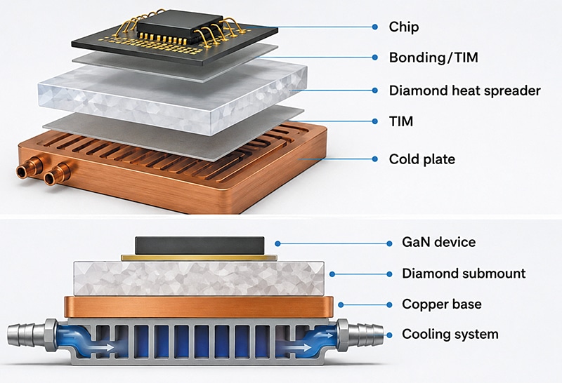
Take a typical package stack: printed circuit board (PCB), substrate, silicon chip, thermal interface material (TIM), copper heat spreader, a second TIM layer, and a cold plate. Diamond can be introduced at several points in this structure. One of the more direct approaches places a diamond plate on top of the chip, separated by thin bonding layers. The diamond sits close to the heat source, where it can pull heat from small hot spots and spread it over a wider area before it reaches the main cooling system.
Diamond can also replace some or all of the copper heat spreader, be bonded underneath a copper lid, or embedded inside the lid to form a diamond-copper structure. Copper-diamond composites are another option, offering thermal conductivity of roughly 800W/m·K, giving designers a choice between single-crystal diamond, polycrystalline diamond, or a composite, depending on the package. It can sit directly below a semiconductor too. In a GaN device, for instance, a diamond submount can go beneath the device and above a copper base plate. Another configuration builds diamond into the package base itself, with a power semiconductor on a ceramic substrate, followed by a diamond-copper base plate and a cold plate. In these layouts, diamond can substitute for copper, aluminium, or silicon carbide, or work alongside them as part of the thermal path.
The benefits are most pronounced where a device produces a lot of heat in a small area. GaN RF flip-chip and diode packaging are strong examples—GaN devices used in radar, satellites, and high-power microwave systems generate high heat densities, and placing diamond beneath the device, or building it into a flip-chip package, helps draw heat away from the active region. In some designs, it can even replace a silicon carbide substrate outright.
High-power laser and photonics packaging are other promising applications. Diamond can be used with laser diode arrays, optical transceivers, and LiDAR systems. Thermal management matters here not just to avoid excessive heat but because even small temperature swings can shift a laser’s output wavelength. So removing heat more efficiently helps keep operation stable.
How diamond is bonded into the package depends on the type of diamond being used. Single-crystal and polycrystalline diamond may require insulating or bonding layers, while a copper-diamond composite can be integrated into the existing package architecture without requiring an entirely new bonding scheme. This may sometimes need only a different surface finish or metallisation.
Diamond surfaces can be metallised with titanium, platinum, or gold to make them compatible with assembly processes, and existing materials such as silver-indium solder or conductive epoxy may still be used, particularly in thermally less demanding applications. In a package built around a chip, solder, and a gold-plated submount, for example, the submount alone could be swapped for a gold-metallised diamond version while the solder stays the same, making diamond, in some cases, a fairly simple drop-in replacement.
| Companies Working on Scientific Applications of Diamonds | |
| Company | Focus |
| Diamfab | Diamond semiconductors, including diamond wafers, Schottky diodes, FETs, power electronics, and quantum applications. |
| Element Six | Part of De Beers Group, develops synthetic diamonds for industrial and high-tech applications, including thermal management, photonics, sensors, and quantum technologies. |
| Kara | Develops engineered single-crystal diamond for thermal management, power electronics, quantum sensing, photonics, quantum networks, and research applications. |
Key point: Many companies producing diamonds for industrial applications also serve the jewellery market. Companies focused mainly on scientific and technical uses therefore represent a more specialised segment.
The hard part: growing diamonds big enough and pure enough
So, what makes a large piece of single-crystal diamond difficult to grow? The first hurdle is size: single-crystal diamond for electronics is currently produced in areas around 20×20mm, with 30×30mm near the practical limit today. Crystal quality gets harder to maintain as the size grows.
Then comes purity. For a material meant to move heat efficiently, impurities like nitrogen are unwelcome, since nitrogen atoms interfere with heat transport through the crystal. Boron and other impurities also need to be kept in check, depending on the application.
But how is that control achieved? In CVD growth, it starts with the gas mixture. Controlled amounts of gas can be introduced into the hydrogen-methane feed using mass flow controllers. But the outcome depends on much more than the gas composition alone. Substrate orientation, methane concentration, temperature, pressure, plasma conditions, and growth rate all shape the final crystal, and because these variables interact with one another, changing one can shift the effects of the rest.
That makes detailed characterisation essential after every growth run, turning the process into a feedback loop: grow the diamond, measure its properties, study the results, and adjust the growth conditions accordingly. AI-based analysis is increasingly being used to spot relationships between growth parameters and material properties, helping tighten that loop.
| Can India turn its Diamond Hub into a Tech Hub? |
| • Surat’s advantage. Surat is a major global diamond hub, with around 90 per cent of the world’s diamonds passing through the city’s ecosystem at some stage. • Beyond jewellery. Several Surat-based companies are now working on synthetic diamond applications for industrial and technology markets. • Indian players. Anjali Semicon, SP3 Technologies, Vegasemi Tech, and JB Dianet are among the companies developing synthetic-diamond materials and products for applications beyond jewellery, including semiconductors, thermal management, and so on. • Early opportunity. As these applications develop, Surat’s existing diamond ecosystem could help India build a larger role in the emerging synthetic-diamond technology market. |
Where diamond is already proving itself
Space companies are exploring diamonds for systems with demanding thermal requirements. AI hardware is another major area. As GPUs and other AI chips become more powerful, heat is becoming concentrated in smaller areas, increasing the cooling burden in data centres.
While diamond can move heat away from the chip more efficiently than materials such as copper, the actual improvement depends on the system design, including the diamond’s thermal conductivity, size, and position within the package. There is therefore no single temperature reduction that applies to every application.
Lower junction temperatures also buy devices more thermal headroom: a GPU can hold its performance without running as close to its thermal ceiling, which can ease thermal stress and potentially extend device lifetime. The same effect ripples out to data-centre cooling: when GPUs run cooler, cooling systems don’t have to work as hard, which can reduce reliance on intensive liquid cooling and, potentially, the electricity spent on cooling overall.
For now, thermal management is the clearest semiconductor application for diamond, especially in systems where heat has become the dominant limit on performance.
Beyond cooling: diamond as an active semiconductor
The next frontier is diamond not just as a heat spreader, but as a semiconductor in its own right. Most current work focuses on placing diamond above or below chips to improve thermal management—important, but only part of the picture. The bigger opportunity may lie in developing diamond as an active semiconductor material. Research into reliable diamond-based semiconductor devices, and ways to manufacture them consistently, could push the material beyond cooling duty and into a larger role in electronics.
Nidhi Agarwal is a Senior Technology Journalist at EFY with a deep interest in embedded systems, development boards, and IoT cloud solutions.