Can the evolving semiconductor industry survive a water crisis? The answer may lie in how fabs grow, where they are built, and how they use water.

Who would have thought water would become one of the semiconductor industry’s biggest infrastructure challenges? And yet it became one because making a chip starts with a deceptively simple requirement that the silicon surface must be extremely clean and precisely controlled.
An accidental discovery started it all.
One of the early breakthroughs was in the year 1955, when Bell Labs researchers found that water vapour introduced during high-temperature processing could form a protective layer of silicon dioxide on silicon. The layer helped protect the wafer surface and control how impurities moved into the silicon, becoming an important step in early semiconductor manufacturing.
As chips grew more complex through the 1960s, keeping the wafer surface clean became increasingly difficult. A single microscopic particle, a trace of metal, or leftover chemical residue could ruin a wafer and severely reduce production yields. Consequently, multi-stage cleaning cycles became a mandatory, recurring step throughout the manufacturing process.
This shift elevated water quality to a critical priority. In the mid-1960s, RCA engineer Werner Kern developed what became known as the RCA cleaning process, later published in 1970. The methodology deployed targeted chemical solutions followed by high-purity water rinses to remove different types of contamination from silicon wafers. Ordinary industrial water was no longer viable; the water surrounding the wafers had to be intensely purified to remove ions, particles, and other contaminants that could re-contaminate the surfaces manufacturers worked so hard to clean.
By the 1970s and 1980s, fabs were building increasingly sophisticated water-treatment systems using technologies such as ion exchange, deionisation, and reverse osmosis to produce the ultrapure water needed for manufacturing. As semiconductor production moved towards mass manufacturing, the amount of water required began to grow with it.
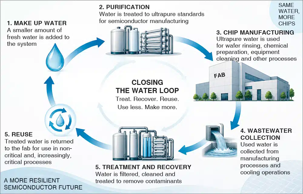
A 1983 US Environmental Protection Agency (EPA) assessment estimated that semiconductor manufacturing facilities in the US were using about 193 million litres of processed water every day. The water was used for wafer rinsing, chemical preparation, equipment cleaning, exhaust-gas treatment, and other manufacturing operations.
At the time, the semiconductor industry had not yet constructed today’s automated mega-fabs or scaled production to billions of hyper-complex chips. Yet, the relationship between water and chipmaking had already fundamentally shifted. Water was no longer just supporting the process; it was becoming part of the process itself.
The efficiency paradox