Tuesday, June 6, 2023

Will 20cm SiC Wafer Be The Next Standard?

By Aarya Padhyegurjar

- Advertisement -
 

Silicon carbide (SiC) has a lot of potential to replace silicon in many applications, a significant one being in the automotive industry, especially for battery-operated electric vehicles. To reduce the cost of producing SiC devices, which is quite high, SiC fabs are moving from 15cm (6-inch) to 20cm (8-inch) wafers.

Porsche Carrera GT uses carbon-fibre-reinforced silicon carbide (C/SiC) ceramic composite braking system

The semiconductor silicon carbide (SiC), commonly known as carborundum, occurs in nature as the mineral moissanite. It is actually abundantly found in space in the form of stardust but occurs very rarely in nature. Nonetheless, since 1893, SiC is being mass-produced for use as an abrasive or in manufacture of light emitting diodes (LEDs) and radio detectors. Today, the ceramics made with SiC, being durable and having high thermal shock resistance, are widely used in automotive brakes and clutches.

Why have we not been using SiC instead of silicon for making semiconductor devices?

- Advertisement -

Earlier, the main problem with SiC crystals was that they had some defects that prevented them from being used widely in electrical applications. Hence, silicon became the standard. However, with technological advancements in production processes, 15cm SiC wafers are now giving a good yield. Particularly in the automotive industry, using SiC instead of silicon can increase the driving range per charge, speed up charging time, and increase efficiency by delivering the same range with lesser battery capacity and weight.

Importance of SiC in automobiles

Today, the electric vehicle (EV) sector is growing rapidly and governments all over the world are taking initiatives for the preservation of the environment. Moreover, petrol prices and CO2 emissions are a matter of great concern. This is why we can see large-scale investments in EVs. Within the next decade, EVs might very well dominate the vehicle market.

But it is important to note that EVs still cannot compete with conventional vehicles in terms of cost—they are significantly expensive. Hence, EV designers and researchers are looking to increase EV efficiency as that will translate to lower costs. Exploring SiCs has pushed EVs towards this goal.

The very properties that SiC has enable it to be used in devices operating at high temperatures and/or high voltages. Automobiles, especially EVs and hybrid EVs, contain many high-voltage systems like the high-voltage battery and its charging sub-systems.

This makes SiC a good choice for use in such applications. With SiC technology incorporated in MOSFETs and diodes, the whole system can be made smaller, lighter, and more efficient.

Electrical systems in EVs, such as battery management systems (BMS) and onboard chargers (OBC), are crucial since the battery is a fundamental feature of EVs. Typically, the OBC is used to charge the battery using AC mains when the car is parked. This is generally a unidirectional process—from mains to the battery. But OBCs can be used the other way round too, for example, when you want to power your home using the energy stored in your EV battery. By using SiCs in such bidirectional chargers, more efficient bidirectionality can be obtained.
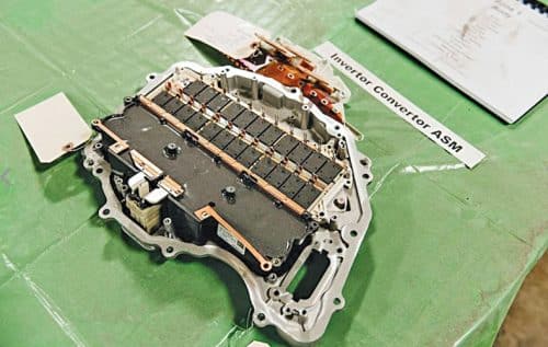
Model 3 main inverter featuring 24 SiC MOSFET modules from ST Microelectronics

Reasons for the success of SiC

According to BusinessWire, “Global SiC market was valued at US$850.6 million in 2020, and is estimated to reach US$2670.25 million in 2007”. Here are some reasons for its success…

[signinlocker id=”87626″]

  • Its on-state resistance and switching losses are considerably lower
  • High thermal conductivity compared to silicon, and hence lesser cooling requirements
  • Allows faster heat dissipation from components
  • Provides high power density, and hence better efficiency
  • Wide bandgap
  • Efficient even in harsh environments due to exceptional hardness and strength
  • Ability to switch at three to five times higher system frequencies
  • High thermal shock resistance and low thermal expansion
  • Chemical inertness because chemical bonds in SiC are stronger

The 15cm to 20cm transition

Many companies have already adopted SiC technology in conjunction with traditional silicon. Tesla, in 2018, added SiC MOSFETs from STMicroelectronics in its inverter for Model 3, due to which the weight of the inverter was reduced by half as compared to other models. The industry believes that although SiC production is not easy on our pockets, the huge demand in the automotive industry will help in decreasing the cost through the economies of scale.

Today, the SiC market is dominated by 10cm and 15cm wafers. Both of these are in high demand, but most of the growth is happening in the 15cm domain, where the aspect ratio of the wafer is 6 to 1. While the industry is looking to improve the methods of processing for 15cm wafers, companies are paying close attention to the development of 20cm SiC wafers at the same time.

The main reason for this transition is to reduce the application cost of SiC. A larger wafer size directly reduces the cost of production. But moving to a larger wafer size is not that easy and establishing mass production infrastructure takes time. Once the mass production of 20cm SiC wafer is established, and the market is no longer dominated by just six to seven companies, the cost of SiC production will drop.

Advantages of 20cm SiC wafers

Ability to produce more SiC devices

20cm wafers can significantly increase the production capacity of SiC devices since a larger area can be used for manufacturing. This will ensure that more devices can be produced using a single wafer of 20cm SiC. Compared to its 15cm counterpart, 20cm wafers will almost double the output of chip production.

Better wafer quality

Approximately twelve wafers are obtained in the batch production of 15cm and 10cm wafers. This number is quite less for 20cm wafers, which is why it is much easier to follow the single-wafer production approach instead of batch production. This enables us to have better control over each wafer, in turn increasing the quality of production.

Electrification

As 20cm SiC wafers become a norm and production capacity increases in the coming years, we can expect major growth in the electrification of systems and products, not just in the automotive sector. The industry might slowly start remaking some fabs that currently run on silicon with SiC technology.

Buck-boost evaluation board for 650V SiC C3M MOSFET (Image source: Wolfspeed)

Disadvantages of 20cm SiC wafers

Need for independent processes and increased investment costs. The production process, as well as the development process of 20cm wafers is fundamentally different from 15cm wafers. Hence, fabrication companies will have to establish independent process plants for the 20cm technology, and this will add to their costs. Not to mention, SiC production itself is more expensive than silicon.

Risk of damages. SiC wafers are already pretty delicate. Developing a wafer of a larger area increases the risk of damaging the wafer during the substrate cutting process. Problems like cutting stress and warpage are evident as the substrate size increases.

Achieving a good tradeoff. Using 20cm SiC will make sense only if the benefits outweigh the challenges, most importantly in terms of cost. For example, the efficiency of the resulting device built on 20cm SiC should compensate for the higher SiC cost as well as the increased costs of 20cm wafer production.

ST’s 20cm SiC wafer
ST’s 20cm SiC wafer

Current trends in SiC industry

Mentioned below are some trends that are being witnessed currently in the silicon carbide industry:

More and more SiC products

So far, several SiC devices have been produced and many have reached maturity as well. For example, many companies, including ROHM Semiconductor, STMicroelectronics, and Infineon, have already launched several SiC based devices like MOSFETs, Schottky diodes, power modules, and hybrid devices. Also, many companies are offering commercially available evaluation kits that feature modules based on SiC.

20cm SiC wafers produced

Due to the cost benefits that the mass production of 20cm SiC will offer, many companies have started the fabrication process of 20cm wafers. Some have already demonstrated 20cm SiC samples. These include Cree (now Wolfspeed), II-VI, SiCrystal (a subsidiary of ROHM Group), and STMicroelectronics.

In July 2021, STMicroelectronics announced that it has manufactured the first 20cm SiC bulk wafers for prototyping next-generation power devices. “The transition to 200mm SiC wafers will bring substantial advantages to our automotive and industrial customers as they accelerate the transition towards electrification of their systems and products,” says Marco Monti, President Automotive and Discrete Group, STMicroelectronics.

5G and SiC

Due to the advent of 5G, there will be demand for high-frequency RF power amplifiers. This is another potential application industry for SiC devices apart from the automotive sector, since GaN (gallium nitride) on SiC is a key technology for 5G power amplifiers. II-IV announced in 2019 that it has introduced prototype 20cm diameter semi-insulating SiC substrates for RF power amplifiers in 5G wireless base-station antennas and other high-performance RF applications.

In-house production

The demand for 20cm SiC is growing and many companies would prefer to produce it in-house. This is why they are expanding their fabrication facilities for the mass production of 20cm wafers. A few years down the line, we can expect several key players in the semiconductor business to have 20cm wafer production facilities.

Bosch aims to become a global leader in the production of SiC chips for electromobility and plans to develop SiC devices on 20cm wafers instead of standard 15cm ones. The company has expanded its wafer fab facilities and is expanding even further for complete in-house production of SiC based devices.

Infineon has been involved in SiC technology for a long time and by 2023 aims to start mass production of 20cm SiC. Cree (Wolfspeed) plans to use existing facilities and install refurbished tools to produce 20cm SiCs in a fiscally responsible manner.

Investments

Another important trend in this industry is the increase in investments in SiC technology. In 2019, Cree (Wolfspeed) announced their largest-ever investment of $1 billion to expand SiC capacity. Moreover, collaborations and acquisitions among semiconductor companies have also become noticeable. Multiple players from all over the world are joining the SiC race and helping the technology become mainstream.

Exciting collaborations

Many semiconductor companies have collaborated, started joint ventures and partnerships in the SiC domain. On 1st February 2022, II-VI Incorporated announced that it has expanded its relationship with GE by signing a three-year technology access agreement (TAA) with GE Research. In November 2021, Japanese power electronics company ROHM and a China based firm known as Zhenghai Group announced a new joint venture that focuses on developing SiC power modules for automotive applications. Many key players in this business have invested in such partnerships with each other.

The future of SiC technology

The competition in the production of 20cm SiC is expected to grow, since the demand for SiC is slowly growing more than the supply. As the automobile industry pushes SiC into the mainstream, most challenges related to 20cm wafers mentioned in this article can be eliminated. However, this will take time, and 15cm wafers might dominate the market for a few more years, after which the 20cm tech will take over. And when this happens, device prices will decrease considerably compared to 15cm SiC.

In a 2005 IEEE paper titled Silicon Carbide Power Devices – Current Developments and Potential Applications, authors Peter Friedrichsi and Roland Rupp mention the following about SiC: “The final market penetration will be somehow related to the fantasy and degree of innovation in circuit design groups, since the simple replacement of silicon by SiC alone cannot justify the cost position resulting from the implementation of SiC.”

Today, not only are SiC devices already in the market, we also have justifiable reasons as to why 20cm SiC wafer might very well become as mainstream in the coming years as 20cm silicon wafer is today.


The author, Aaryaa Padhyegurjar, is an Industry 4.0 enthusiast with a keen interest in innovation and research.

[/signinlocker]


SHARE YOUR THOUGHTS & COMMENTS


What's New @ Electronicsforu.com?

Truly Innovative Tech

MOst Popular Videos

Electronics Components

Tech Contests