


On average, a chip holds over one billion transistors today. Intel’s 10-core Xeon Westmere-EX packs 2.6 billion transistors into a 512mm2 area using 32nm technology. But even that is not enough. The thirst for more features and processing power is unquench-able, but how much more can you pack into a chip? If transistors get any smaller, their reliability could become questionable. Plus, if you need to make chips denser, the fabrication costs might also become unreasonably high.
Such issues have led to the adoption of three-dimensional (3D) integrated circuit technology, wherein two or more dice are stacked atop each other and linked with suitable interconnects. You can draw a parallel with skyscrapers, which help overcome space shortage within large cities, and elevators that make it possible for people and even vehicles to easily travel to any of the floors.

What are the main benefits of 3D chips?
1. 3D chips save space. Dice that used to be centimetres apart on a chip can now be placed millimetres apart, and that too vertically.
2. Since the dice are close by, the interconnect length is significantly smaller. This results in low latency and higher performance.
3. Stacking helps overcome the memory-to-processor performance bottleneck that plagues 2D ICs.
4. 3D interconnects permit data to be moved both horizontally and vertically. This helps boost performance by 30 to 40 per cent.
5. Bandwidth is much higher as it is possible to have a large number of vertical vias between the layers. Moreover, interconnects between dice in the 3D IC do not use input/output (I/O) buffers or bond wires.
6. 3D chips consume 40 to 50 percent less power than traditional ICs.
7. 3D stacking permits heterogeneity, since the dice arranged one above the other need not be similar. This allows a designer to optimise components according to their function.
Are today’s ‘3D’ chips really 3D?
There is a difference between a 3D package and a 3D IC.
In a 3D package, separate chips are stacked in a single package. They may be stacked one above the other or side-by-side. This arrangement is often called a chip stack, system-in-package (SiP) or multi-chip module (MCM). Here the chips are merely stacked and connected using interconnects but not integrated into a single chip.
In contrast, a 3D IC is a single chip. Multiple dice are stacked, connected using through-silicon vias (TSVs), and multiple groups of dice again connected together using a silicon interposer—and all of this is mounted on a single SiP.
3D chips are in development stage, and any chip touted as 3D today is essentially a 2.5D chip or a 3D package as most of the commercially-available or practicable designs today are MCMs or package-on-package. Pure 3D ICs (stacking in package) are still a point of research in most companies, and the big foundries have just figured out the processes and interposer technology for the same.
Although Intel has showcased quite a few 3D ICs in the past, such as the 3D Pentium CPU in 2004 and the Teraflops Research Chip in 2007, the area continues to haunt the silicon giant because of the difficulty in heat dissipation and the high cost of manufacturing involved. This year too, 3D-IC-based multi-core designs using GlobalFoundries’ 130nm process and Tezzazon’s FaStack technology were demonstrated at a leading conference, as also some designs by teams from the Georgia Institute of Technology and the University of Michigan. However, it is unclear when the technology might actually reach production.
Techniques for stacking the dice in a 3D chip
There are several ways to stack chips. Giles Peckham, EMEA director-Marketing, Xilinx, explains the most common ones:
1. Connecting two stacked chips to a flip chip at the bottom of the stack. Examples are SoCs where dynamic random-access memory (DRAM) is placed on top of the central processing unit (CPU).
2. Using TSV, where the dice are placed on top of each other and connected through vertical copper channels. An example of TSV usage is the super-density DRAMs used in camera CMOS sensors.
3. Making use of a silicon transposer, which connects two or more chips together—much like the transposers used in AMD graphics cards.
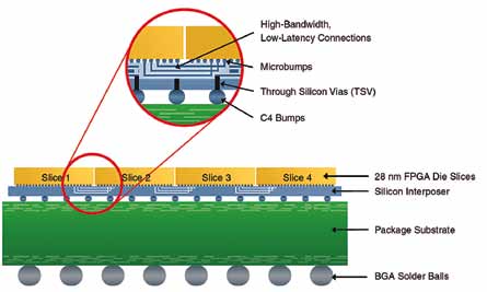
Xilinx adopts a technology called stacked silicon interconnect (SSI). In this architecture, multiple dice are placed side-by-side on top of a passive silicon interposer, which facilitates interconnect/communication between the many dice. Such a design, where the chips are placed side by side, is called a multi-chip module but should not be confused with a traditional MCM in which the connections between the chips are made via powerful I/O buffers and bond wires. In SSI technology, the connections are virtually seamless, the interposer being an extension of the on-chip interconnect with microbumps to join them. With more than 10,000 interconnects that can be programmed among the dice, and programmability of each die and the I/O, the company claims its ICs to be one of the first commercially-available, completely-programmable 3D ICs.
Texas Instruments has an alternative technology, called PowerStack, for 3D packaging. It involves stacking TI’s NexFET power MOSFETs on a grounded lead frame and connecting them using copper clips. This combination of stacking and clip bonding results in a more integrated quad flat no-lead (QFN) solution that delivers a smaller size, better thermal performance, higher switching speed and higher current capabilities over more traditional solutions that utilise MOSFETs placed side-by-side.
[stextbox id=”info”]Pure 3D ICs (stacking in package) are still a point of research in most companies, and the big foundries have just figured out the processes and interposer technology for the same[/stextbox]
Challenges before the industry
First, there is the issue of thermal flux. “Stacking multiple active dies directly on top of each other leads to high concentrations of heat which cannot easily be dissipated,” explains Peckham.
SSI technology places active silicon side-by-side with active silicon on top of passive silicon, thus avoiding the thermal flux issues. While this is workable in MCMs, it is still a daunting issue in true 3D chips. IBM, along with 3M, is working hard to overcome this problem.
Since there are many extra steps involved in manufacturing 3D ICs, the possibility of defects introduced in each step is also high. Yield might be lower than for 2D chips.
Testing of independent dice is relatively tough because of the tight integration between active layers. This introduces further possibility of defects going undetected.
Since 3D TC is a new technology, design is relatively complex, and comparatively fewer tools are available.
Also, there is still no consensus on the methods of design, manufacture, testing and manufacturing of 3D ICs. Plus, there are several integration options—via-last, via-first, via-middle, interposers, direct bonding, etc. Hence there are very few standards governing the 3D IC lifecycle, making it very difficult for all stakeholders.
There is also a bit of confusion about how Internet protocol (IP) will have to be characterised to work effectively in stacked-die configurations.
Are 3D chips in production today?
Some or the other forms of 3D stacking has been in use for many years, especially for stacking memory chips. Irvine Sensors Corporation, for example, has been stacking chips for space electronics for the last 20 years. The company also stacks relatively lowpower chips (often memory) for cell phones and consumer products, where small size is needed. However, past examples have always been simple designs, and not done full justice to the benefits of 3D stacking. More complex designs have so far been tough to implement due to heat dissipation issues, cost of manufacture, interconnect technologies, etc.
Now, after years of research, companies are finally figuring out practical ways to manufacture MCMs and package-on-package designs if not stacking-in-package ICs:
1. Xilinx claims to have utilised SSI technology to create the industry’s largest FPGA (Virtex-7 2000T) with a capacity of two million logic cells, and the world’s first heterogeneous 3D FPGA (Virtex-7 H580T) with high-speed 28Gbps serial transceivers. Both are being sold worldwide and used in applications including ASIC prototyping, storage and high-performance computing systems.
“It has taken many years for Xilinx to combine a number of proven manufacturing techniques used by industry-leading partners to create the complete SSI technology manufacturing process and to bring it to a production-ready state. We have been shipping the devices to many customers around the world for about a year now and in 2012 we started to ship our first heterogeneous devices. SSI technology in 3D devices today makes feasible what would otherwise be impossible in a 2D (monolithic) device. Cost is therefore not the primary driver for these applications today but 3D ICs will inevitably migrate down the cost curve as volumes and experience increase over time,” says Peckham.
2. Texas Instruments’ PowerStack technology is being put into production at its state-of-the-art Clark facility, where many of TI’s analogue products go through assembly, packaging and test. The facility also has the capacity for qualifying QFN.
3. TSMC, which is developing TSV technology (called through-transistor substrate within the company), is likely to start commercial 3D chip production in 2013. Last year, there were some reports about Apple basing its A6 processor on TSMC’s 28nm plus 3D stacking technology, but there has been no official announcement yet. Altera is also a TSMC collaborator.
4. Applied Materials Inc., along with the Institute of Microelectronics in Singapore, has set up an advanced 3D chip packaging facility at a cost of $100 million.
5. Samsung apparently has a good 3D packaging technology for memory chips.
6. GlobalFoundries plans to start production around 2014. Although industry giants like Intel and HMC have the technology to fabricate 3D ICs in-house, they have still not started production.
7. Finding true-3D IC manufacture very costly, Intel has started producing chips based on its novel Tri-Gate technology that makes use of 3D transistors. This technology is apparently just 2 to 3 per cent costlier than traditional designs while offering many of the benefits of 3D ICs.
Speaking at the Intel Developer Forum this year, Mark Bohr, Intel’s Process Guru, revealed that Intel is still studying ways to implement true 3D ICs, but sounded sceptical about the chances of the firm implementing it.
“Having the technology and having a cost-effective solution are two different things,” Bohr said. “We can do 3D chip stacking, but I think the added cost is still a bottleneck.”
Bohr added that multi-chip packages and package-on-package technologies are already in wide use and appear to be far more cost-effective than 3D chip stacking.
“The problem with 3D stacking is that it may be a viable solution for a 1-watt product, but it’s not an acceptable solution for a 30- or 40-watt product because you can’t dissipate all of that heat out of the package,” Bohr said.
8. Meanwhile, IBM is planning an alternative route for manufacture of 3D ICs. It believes that the best way is to glue together entire wafers with a thermal adhesive it has developed in collaboration with 3M. Apparently, doing the tricky alignment once and then dicing apart the wafer might be less expensive than stacking tiny chips after they have been diced out of the wafer.
9. Hewlett-Packard is working to create stackable 3D chips that communicate using built-in microscopic lasers. These chips consume 80 per cent less power than traditional chips and are targeted for release in 2015.
What design tools are available to start using 3D chips?
Peckham pushes designers to try 3D, saying, “3D chips enable designers to create system-level designs with unprecedented levels of integration, leading to higher performance and lower power consumption than has ever been possible before.”
Depending on the chips they plan to use, designers can choose from various toolkits to design their computing systems using 3D chips. Some experts feel that a toolkit need not be purely 3D, but a generic one which is 3D-aware.
[stextbox id=”info”]3D chips enable designers to create system-level designs with unprecedented levels of integration, leading to higher performance and lower power consumption than has ever been possible before[/stextbox]
To improve designers’ productivity with its all-programmable devices at 28nm and beyond, Xilinx has developed a next-generation design environment and tool suite called Vivado. Without this design suite, design teams could not effectively leverage Xilinx’ 3D ICs. The Vivado Design Suite further improves the quality of designs by up to three speed grades, cuts dynamic power consumption by up to 50 per cent, improves routability and resource utilisation by over 20 per cent, and speeds time to integration and implementation as much as fourfold.
Design automation leaders like Cadence, Mentor Graphics, Synopsis and Calypto have several tools for 2.5D as well as 3D IC design. Synopsis has teamed up with TSMC, while Cadence has collaborated with Taiwan’s Industrial Technology Research Institute to design next-generation 3D ICs.
TSMC also works with tools from Apache Design and its parent company ANSYS for its 20nm and stacked die reference flows, as these tools address thermal analysis, run-away and thermal-induced electromigration, as well as power, noise and reliability issues. The tools include RedHawk, Totem, Chip Thermal Model, Sentinel-TI, Slwave and Icepak. It is important to use tools that address multifarious issues rather than focus only on performance aspects.
The author is a technically-qualified freelance writer, editor and hands-on mom based in Chennai
