Chirality and CNT types
Chirality is related to the degree of twist of the tube’s lattice and can be described by chiral vector. Chiral vector is a circular vector that is perpendicular to the axis of the tube. It is a linear combination of base vectors ‘a1’ and ‘a2.’ Nanotubes form different types, which can be described by chiral vector (n, m), where ‘n’ and ‘m’ are integers of vector equation Ch = na1 + ma2.
Values of ‘n’ and ‘m’ determine chirality, or ‘twist’ of the nanotube. As a thumb rule, a CNT is metallic if (n-m)=3K, where ‘K’ is an integer. Otherwise, it is semiconducting. Consequently, when tubes are formed with random values of ‘n’ and ‘m,’ statistically two-thirds of nanotubes are semiconducting, while the other third are metallic.

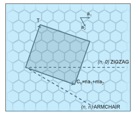
Two special kinds of CNTs are defined as the zigzag CNT when m = 0, and the armchair CNT when n = m. CNTs other than these two special kinds are generally referred to as chiral nanotubes.
Chirality, in turn, affects the conductance, density, lattice structure and other properties of the nanotube. Depending on its chirality, a tube can be classified as either semiconducting (presence of a band gap) or metallic (absence of a band gap). This property of CNTs stems from the electronic structure of graphene. The energy band gap can be varied by varying the magnetic field along the axis.
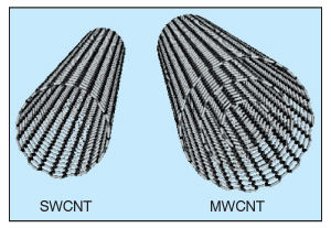
Nanotubes with one layer of carbon atoms are referred to as single-wall (SWCNTs), while those with multiple layers are called multi-wall (MWCNTs). Metallic nanotubes are used as Coulomb islands in single-electron transistors, whereas semiconducting nanotubes are used as the channel in field-effect transistors. Metallic CNTs show very low-resistance, high-current-driving capabilities and almost no heat dissipation—features that can be exploited to build high-performance interconnections and devices for integrated circuits.

CNTs may also display different behaviours depending on whether they are single-walled or multi-walled. Thus SWCNTs can be thought of having the fundamental cylindrical structure, which forms the building blocks of multi-wall nanotubes, the arrays of single-wall nanotubes and CNT bundles.
CNT conductance
The resistance to conduction is determined by quantum mechanical aspects and is independent of the nanotube length. Theoretical studies have revealed that the optical activity of chiral nanotubes disappears if the nanotubes become larger. Detailed treatment of CNT electronics requires an atomistic description of the nanotube along with a quantum-mechanical treatment of electron transport. For ballistic transport, we self-consistently solve the Poisson and Schrödinger equations using the non-equilibrium Green’s function (NEGF) formalism.
CNT reactivity is directly related to the pi-orbital mismatch caused by an increased curvature. Therefore a distinction must be made between the side wall and the end caps of a nanotube. For the same reason, a smaller nanotube diameter results in increased reactivity.
CNTs have a very large Young’s modulus in their axial direction. The nanotube as a whole is very flexible because of its great length. CNT growth involves interaction between nanotubes and substrate surfaces. This interaction is so strong that it can influence carbon nanotube growth such as length and position.
The conduction and valence bands are symmetric, which is advantageous for complementary applications. The band structure is direct, which enables optical emission and, finally, CNTs are highly resistant to electromigration.
CNT diameter and band gap
When the diameter of a CNT is changed, it causes a change in power delay product. Leakage power increases when the diameter is increased. Even though the current in a CNT is smaller than for a minimum-sized MOSFET (at 32 nm), the CNT has a steeper curve in the transition region due to the higher gain. This contributes to a 22.5 per cent improvement in noise margin; this improvement in performance is reflected in decrease in power supply voltage.
The band gap is inversely proportional to the diameter of the nanotube as per the following relationship:
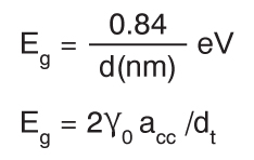
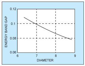
where ‘γ0’ is the carbon-to-carbon tight-binding overlap energy, ‘acc’ the bond length of carbon atoms and ‘dt’ the tube diameter. Typically, a semiconducting SWCNT has a diameter of 1.4 nm and a band gap of about 0.5-0.65 eV. The energy gap of semiconducting CNTs can be varied continuously by varying the nanotube diameter. Here the band gap of semiconducting nanotubes decreases with increasing diameter.
A few facts about CNTs
The operation frequency is limited due to parasitic capacitance and huge external resistance. High ‘off’ current and large leakage are big issues considering the power consumption. SWCNTs result in major concentrations of impurities. These impurities are typically removed by acid treatment, which introduces other impurities that can degrade nanotube length and perfection, and adds to nanotube cost. These types of resistances are very important and can dominate electrical transport in nanotubes, especially at low temperatures where typically they lead to charging and the observation of Coulomb blockade phenomena.
Major sources of disorder in nanotubes are localised lattice defects, such as vacancies, substitutions, pentagon-heptagon defects and hetero-junctions between nanotubes of different chiralities. Such defects are typically formed during nanotube growth, by volatile processing or by intentional damage. The atomically sharp nature of these defects leads to large momentum scattering.
Electrostatic potential fluctuations, created by a random distribution of charges in the substrate by molecules adsorbed on the nanotube or by processing residues, can induce both short- and long-range disorder. Mechanical deformations include local strains and twists, which affect the local band gap as well as kinks that act as conductance barriers.
CNTs possess two kinds of inductances, the magnetic (or mutual) inductance and the kinetic (or self) inductance. Kinetic inductance dominates mutual inductance in a 1D structure like CNTs and hence we only consider kinetic inductance in the model. CNTs have two modes of propagation, with two electrons in each mode (spin up and spin down). Larger diameters have a higher leakage and are harder to switch off. Smaller diameters have a 5x decrease in speed than larger-diameter CNTs.
The reason for the usage of atomic force microscopy (AFM), transmission electron microscopy (TEM) and scanning electron microscopy (SEM) in nanotubes analysis is very simple. AFM is a powerful tool in manipulating and characterising the topography of nanostructures. TEM has been traditionally applied to characterisation of the interior structures of nanomaterials. Scanning electron microscope with high resolution is a powerful instrument for imaging of fine structures and morphology at high magnification.
To sum up
The integration of CNTs can be achieved in micro/nano electronic devices if we manage to fabricate nanotubes of particular type, length and diameter in optimised manner. The interdisciplinary science of CNT can be well understood for application in electronics. Though the process is still at embryonic stage, in the near future we will achieve the goal of fruitful integration in electronic devices.
Subhranshu Sekhar Samal is a Scientist-D at Centre for Nanoscience & Nanotechnology (a joint initiative of IGCAR, Kalpakkam, and Sathyabama University, Chennai), Sathyabama University, Chennai. He has more than seven years of research experience in nanocomposites and nanomaterials. Prof. Greeni Navin is an assistant professor in Department of ECE, KNS Institute of Technology, Bengaluru. Her current focus is understanding the nanomaterials and researching different parameters that can enhance the functioning of nanodevices