


A semiconductor sits at the heart of any electronic device. Over the last few years this industry has witnessed a boom that is revolutionary in many ways due to the digitalisation of various electronics prospects along with the advancements that one could not have expected a decade ago. Read on to learn more about the same
Digitalisation is the representation of the fundamental changes in the business landscape. It includes the aspects of putting increasingly smart systems in place, which are capable of being reconfigured on the fly and delivering new and unprecedented user experience, and how companies are digitalising their whole business operations.
Increasingly, companies are moving more of their business fabric onto a semiconductor framework, which is enabling them to move from an on-site premise work environment to distribute the work around the globe. If you go look out in the market today, you will see some of the following trends settling in.
Increasing semiconductors content
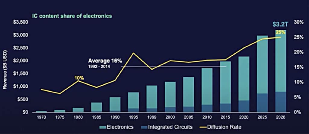
We can see in the chart in Fig. 1 that the semiconductors content in electronics is increasing steadily. Historically, during the mid-90’s this growth was at a fairly constant level of about 16% of the overall electronics. Considering the rate at which we are putting out new smart systems with greater abilities, by the year 2026 about 25% of those machines will drive off semiconductors, hence paving opportunities for the companies involved in this space.
Companies becoming SoC designers and manufacturers
Increasingly the systems houses are becoming IC design companies as well. This trend has been witnessed in the smartphone space, whether it is Apple, Google, or others. Companies working in this space have increasingly started designing their own ICs. Even in communication and automotive sectors the original equipment manufacturers are increasingly becoming designers rather than mere consumers of semiconductors.

System companies growing
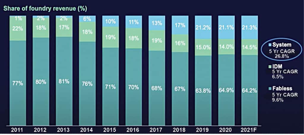
The chart in Fig. 2 shows the percentage of the foundry customer revenue coming from the traditional integrated device manufacture (IDM) companies and from the new system companies. A decade ago, the systems companies were a trivial part of the foundry revenue. It has now increased and is likely to be about 21.3% next year, which represents a compounded annual growth rate of almost 27%. A lot of that has been in the areas such as Apple’s iPhone but this trend is becoming common as these systems companies take more and more control over the architecture to deliver a better experience for their customers.
The four trends driving the digitisation strategies for these companies are sensors, edge computing, 5G/wireless communications, and cloud/data centres. Sensors provide the ability to digitalise the natural world and bring that into a compute infrastructure for new types of applications. Edge computing enables integration of devices into smaller footprints while allowing application of things like machine learning and artificial intelligence within those chips. 5G provides an infrastructure that enables pulling these devices together. Cloud and data centres allow taking this final set of data and deliver the end applications to the customers.
The chart in Fig. 3 compares the number of sensors linked to the internet in 2015 versus the number likely in 2025. As you can see, in 2015 there were about 1.6 billion sensors and by 2025 their number is projected to be almost 30 billion.
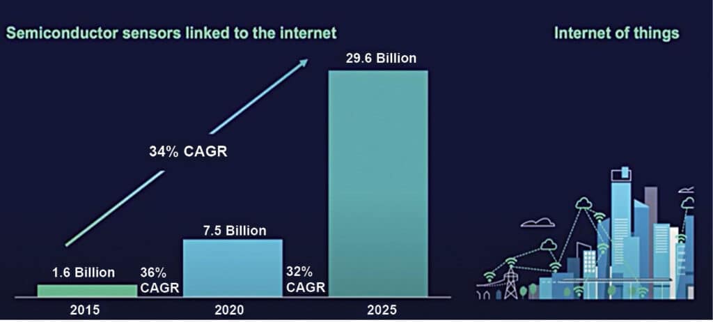
Fig. 4 shows a strong growth opportunity for 5G, which is expected to grow at about an 18% rate over the next few years. It also shows that consumer/compute, automotive, industrial, and infrastructure/other wireless applications are going to be an even larger driver of this opportunity as people start connecting those sensors and move that data into the data centres.

The chart in Fig. 5 shows a significant increase in growth and opportunities in data centres themselves. It shows a strong recovery from the dip in 2019 due to move to a virtualised work environment because of the pandemic. For the next five to six years the increase is likely at the rate of 11% CAGR in that large market, driving towards a 14% CAGR in later part of the decade.
Semiconductor market growth
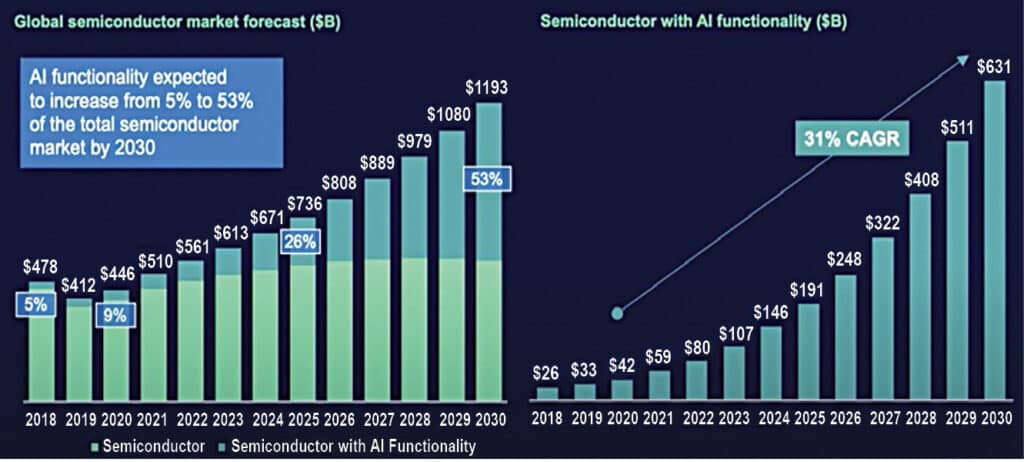
The chart in Fig. 5 shows semiconductor growth moving forward. The chart on the left shows predictions that seem to be lining up these days for a trillion dollar semiconductor market around the year 2030. It can be seen that there is significant difference between baseline semiconductors and the semiconductors that have AI functionality.
At present, about 10% of the chips being produced have some sort of AI in them. Notable examples are cellphone application processors that have AI engines to do things like facial recognition. About half of the market will be represented by chips with AI by 2030.
Explosion in global funding
The first thing to look at is venture capital (VC) investments (see Fig. 6). Before the dot-com crash, the VC investments were about 2.5 billion dollars, which dropped by about 40% after the crash to about 1.7 billion dollars for a few years. In 2009, the great recession dropped that down further to under 1 billion dollars a year, which were being spent on semiconductor content. It continued to fall until 2015, when it eventually dropped to half a billion dollars. Thereafter, the investments picked up sharply and in 2021 we had almost 10 billion dollars investment flowing into startup companies in the semiconductor space.
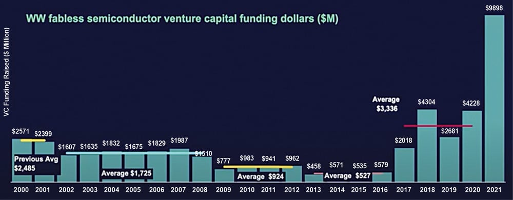
Previously, the majority of the spending was being done in the United States (US) alone but now this trend has spread globally. China, with its well-known effort to become an important provider in the semiconductor space, has led with almost 6.5 billion dollars of spending. But even the rest of the world, outside of the US and China, has made about 1.6 billion dollars of investment into those semiconductor companies. This trend is expected to increase further as more and more nations are realising the strategic importance of semiconductors for enabling their overall economic growth.
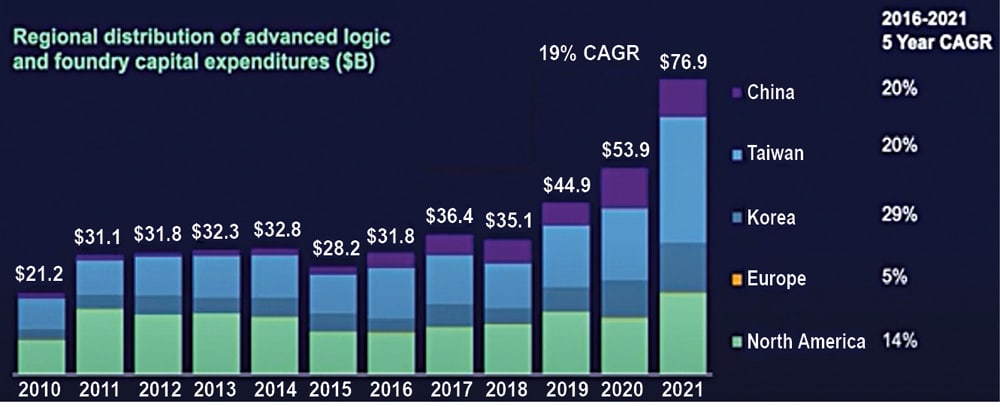
Advanced logic and foundry capital investments
The chart in Fig. 7 shows the distribution of advanced logic and foundry capital expenditure. It can be seen that was a relatively flat spending until about 2018. It started increasing from the year 2019 and reached close to 80 billion dollars in 2021. Taiwan Semiconductor Manufacturing Company (TSMC) has already stated that they will spend approximately 40 billion dollars on enabling new foundry capacity next year. So, we can expect to see a significant increase in this number in the future.
Announcement by the Indian government
The government of India announced approximately 10 billion dollars of incentives for the electronics and semiconductor industry on 21st December last year, which was particularly encouraging for the industry. There are schemes for putting semiconductor fabs in place, schemes for putting compound semiconductor fabs, schemes for lower-end fabs as well as assembly and test, and, finally, schemes to work towards increasing design capacity within the country.
EDA for design activity
In the field of electronic design automation (EDA), there is an encouraging trend for India. In the last ten years worldwide, the spending on EDA has been increasing at about 9%. In India it has increased at 12% CAGR. This indicates that design activity for the global semiconductor industry, which has been done largely within India, also provides a good platform on which the future semiconductors can be built.
Semiconductors are becoming a critical part of implementing not just near-normal electronics but also the companies’ infrastructure and how they present themselves to the world. The three pillars for enabling digitalisation for outsized growth are:
Technology scaling. One of the fundamental benefits of people implementing this digitalisation is the fact that we can continue with Moore’s Law, scale technology, and deliver more functionality at the same cost over time, which enables them to transform themselves and have a very positive future.
Moore’s Law also has a dark side. Twice as many transistors can be produced every two years which will, in turn, require twice as many transistors to be used as well. Hence, we need to put new methodologies in place that enable us to do so.
System scaling. The application needs to get validated across the semiconductors before these are produced to ensure that overall the application can fit within the parameters it has. Also, it needs to provide the user experience it is expected to deliver in an environment where there is a sensor driving an edge computer that would work through 5G to the data centre.
Enabling technology scaling
The chart in Fig. 9 for Apple’s domain-specific processor evaluation shows an eight-year time horizon, which is equivalent to four Moore’s Law cycles. It shows that in the year 2013, the A7 processor had approximately a billion transistors while in 2021 the A15 had approximately 15 billion transistors. It is almost exactly on the schedule that you would expect from Moore’s Law.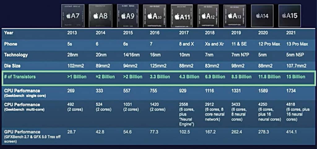
These chips perform efficiently as well. The A7’s Geekbench single central processing unit (CPU) score is 269 while for the A15 the score stands at 1734. This increase in score is mapped against multi-core performance as well as the graphical processing unit (GPU) performance.
Cost scaling with design scaling
If we were to estimate the amount of tape outs that occur per year and do any kind of matrix multiplication of tape outs per node against this, we will quickly run out of money in the industry. We as a company are currently doing a seven manometer (7nm) chip. The trend line is mapped well whether the numbers are exactly correct for any particular chip or not.
It becomes increasingly more expensive to do design as we move down these technology nodes. The design cost does not double, so the design cost per transistor continues to be cheaper.
The history of the EDA industry has been about increasing layers of abstraction. Back in the eighties, a tremendous amount of work was done at the transistor and SPICE (a general-purpose, open source analogue electronic circuit simulator software used in IC and board-level design to check the integrity of circuit designs and to predict circuit behaviour) level. In the late eighties and early nineties, the transition to RTL occurred. The transition to RTL enables us to design more quickly.
Understanding PAVE360
Siemens introduced a simple but revolutionary pre-silicon autonomous validation program, PAVE30, in May 2019 to accelerate the development of autonomous vehicle platforms. It provides an environment for multi-supplier collaboration across the automotive ecosystem for the development of automotive chips.
PAVE360 also extends digital twin simulation beyond processors to include automotive hardware and software sub-systems, full vehicle models, fusion of sensor data, traffic flows, and the simulation of smart cities through which self-driving cars will ultimately travel.
We have a sensing environment where we can model scenarios of real world data to where you can put traffic lights, traffic lanes, pedestrians, and other vehicles, all in place that allows you to run these various scenarios and then produce sensor data that can be virtualised and fed into the compute and analysis function.
This article is based on a tech talk at VLSI 2022 by Joe Sawicki, Executive Vice President, Siemens Digital Industries Software. It has been transcribed and curated by Laveesh Kocher, an EFY tech enthusiast with a knack for open source exploration and research.
Joe Sawicki is Executive Vice President at Siemens Digital Industries Software