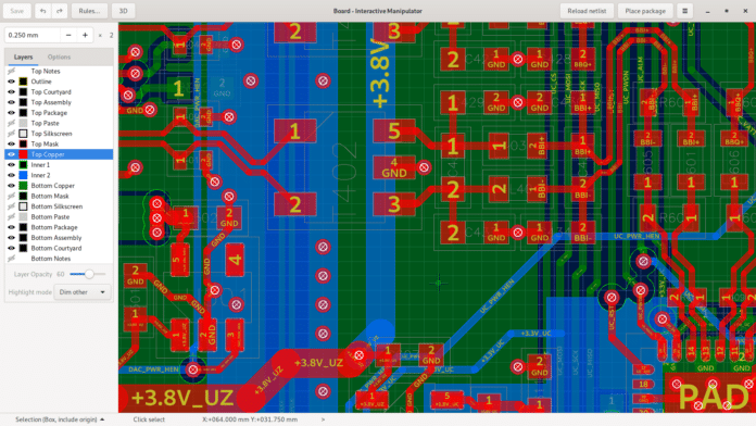

Design, check, and prepare PCBs for manufacturing with a free open-source tool built to simplify the entire electronics design workflow from start to finish.
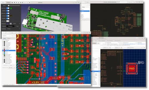
Horizon EDA is an open-source electronic design automation (EDA) software that provides a complete workflow for printed circuit board (PCB) design. It covers everything from library management and schematic capture to PCB layout, design rule checking (DRC), bill of materials (BOM) generation, PDF export, 3D board viewing, and export of Gerber and NC-Drill manufacturing files.
The software was designed with simplicity as its main principle. Instead of using complex class hierarchies, its developer chose a straightforward core data model with a direct relationship between the user interface and the underlying design data. This approach helped reduce software complexity, simplify maintenance, and minimise bugs.
Development followed a breadth-first strategy, where basic versions of all major modules were built before refining individual editors. This allowed the overall architecture to be tested early, user feedback to be incorporated throughout development, and older code to be replaced when better approaches were found.
Horizon EDA also includes a multi-threaded design rule checking tool to identify common PCB design errors. It supports touchscreen gestures such as pinch-to-zoom and direct manipulation of both 2D and 3D views, works with modern laptop pointing devices for precise navigation, and allows users to customise the interface, including choosing different colour schemes.
Horizon EDA does not have separate free and paid editions. It is completely free and open-source, meaning all users have access to the same set of features without requiring a subscription or license fee. “If you’re looking for an EDA tool with a fresh approach to PCB design, Horizon EDA is worth exploring. It takes a different design philosophy that makes the overall workflow simpler and more intuitive,” said on user.
What can you do with Horizon EDA?
Engineers can use Horizon EDA throughout the PCB design process, from creating schematics to generating manufacturing files. It is suitable for electronics professionals, hardware developers, makers, researchers, and students working on circuit and PCB design.
They can use Horizon EDA to:
- Create circuit schematics for analog, digital, mixed-signal, and power electronics projects.
- Design PCB layouts, including component placement and trace routing for single- and multi-layer boards.
- Build and manage component libraries with reusable symbols, footprints, and 3D models.
- Run design rule checks (DRC) to identify clearance, connectivity, and layout errors before manufacturing.
- Generate manufacturing files, including Gerber files, drill files, pick-and-place files, and bill of materials (BOM).
- View and export 3D PCB models to inspect board assemblies or use in mechanical CAD workflows.
- Manage parts using project pools, allowing components and libraries to be shared and updated across multiple projects.
- Prepare designs for assembly by generating placement and production documentation.
- Export documentation such as PDFs, fabrication drawings, and assembly outputs for manufacturers and collaborators.
- Develop open-source hardware projects, as the software itself is open source and supports customizable design workflows.
Who Can Use Horizon EDA?
| User | What They Can Do with Horizon EDA |
| Students and hobbyists | Learn schematic capture, PCB layout, and library creation while building educational or personal electronics projects. |
| Electronics engineers | Design analog, digital, mixed-signal, power, and embedded system PCBs, run design rule checks (DRC), and generate manufacturing files. |
| PCB designers | Create single- and multi-layer PCB layouts, define design rules, route traces, create copper pours, and prepare boards for fabrication. |
| Hardware startups and product developers | Develop prototypes, manage reusable component libraries, generate bills of materials (BOMs), and prepare designs for production. |
| Open-source hardware developers | Build and maintain shared component libraries, collaborate using Git, and automate design tasks with Python scripts. |
| Researchers and educators | Develop custom hardware for research, teaching, and academic projects using an open-source PCB design platform. |
Design Workflow in Horizon EDA
Horizon EDA follows a structured workflow that takes a design from concept to manufacturing. Each stage is integrated, making it easy to move from circuit design to a production-ready PCB.
- Set Up the Component Pool
Start by selecting an existing Pool (library) or creating your own. The Pool contains symbols, footprints, parts, and other reusable design elements needed for the project. - Create the Schematic
Draw the circuit by placing components from the Pool and connecting them with wires and nets. Add power symbols, labels, and annotations as needed. - Assign Footprints
Link each schematic symbol to its corresponding PCB footprint so the components can be placed correctly on the board. - Generate the PCB
Create a PCB layout from the completed schematic. Components are transferred to the board along with their electrical connections. - Define the Board Outline
Draw the physical shape and dimensions of the PCB, and configure the required number of layers and board settings. - Place Components
Arrange components on the PCB while considering signal flow, mechanical constraints, thermal requirements, and manufacturability. - Route the Board
Connect the components by routing traces. Horizon EDA supports interactive routing, differential pair routing, copper pours, and length tuning where required. - Run Design Rule Checks (DRC)
Verify the design by checking for issues such as clearance violations, unconnected nets, and other rule violations. Errors can be corrected before manufacturing. - Review the Design in 3D
Inspect the completed PCB using the integrated 3D viewer to verify component placement and mechanical fit. STEP files can also be exported for integration with mechanical CAD software. - Generate Manufacturing Files
Once the design is verified, export the files required for fabrication and assembly, including Gerber files, NC Drill files, Bill of Materials (BOM), pick-and-place files, and PDF documentation. These files can be sent directly to a PCB manufacturer and assembly service.
What’s New?
The latest stable release of Horizon EDA, Version 2.7.2 (December 2025), focuses on improving usability, simplifying project management, and fixing several issues affecting PCB design workflows.
- Simplified project pool updates: The software now automatically detects changes in the project pool and prompts users to update the cache with a single click, eliminating the need for manual reloading.
- Reusable pick-and-place export settings: Users can now save and load pick-and-place export configurations, making it easier to reuse the same settings across multiple projects.
- Package parameter locking: Packages can now have fixed parameters, helping prevent accidental changes to package dimensions during design.
- Improved silkscreen rendering: Fixed an issue where bottom-side silkscreen arcs were not rendered or exported correctly.
- Correct PDF export scaling: Resolved a bug that caused images in PDF exports to appear at incorrect sizes.
- Better Windows compatibility: Fixed problems importing DXF files with non-ASCII characters in their filenames on Windows systems.
Advantages and Limitations
Horizon EDA offers a complete PCB design workflow in a free and open-source package, making it suitable for students, hobbyists, and professional engineers. It includes schematic capture, PCB layout, real-time design rule checking (DRC), integrated 3D visualization, and manufacturing file generation without restrictions on board size or project complexity. A key feature is its Pool-based library management system, which simplifies component and footprint creation, reuse, and version control. The software also supports Git integration for hardware design collaboration.
However, Horizon EDA has a smaller user community than more established PCB design tools, so there are fewer tutorials, third-party libraries, and community resources. It supports Windows and Linux but does not have a native macOS version. It also lacks built-in circuit simulation, such as SPICE, and is focused on PCB design rather than FPGA or integrated circuit (IC) development. Some advanced workflows and integrations available in mature commercial EDA tools are also not yet supported. “Conceptually, Horizon EDA is much simpler to use. However, it has a few limitations. For example, it may not automatically recognize multiple connector pins that are internally connected, requiring them to be connected manually,” added one user.
Supported Platforms and File Formats
| Category | Supported Options |
| Operating Systems | Windows, Linux |
| Import Formats | KiCad footprints, DXF artwork, IBIS models |
| Export Formats | Gerber (RS-274X), NC Drill, STEP, Bill of Materials (BOM), Pick-and-Place files, PDF documentation |
| 3D Support | Real-time 3D board viewer, STEP model import, STEP export for mechanical CAD |
| Library Support | Horizon Pool libraries, Project-specific Pools, Shared Pools, Git-managed libraries |
Click here for more information.