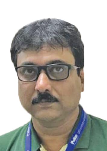
High-speed PCB circuits have wide-ranging applications from medical equipment to network communication. Amit Bhardwaj, group chairman and managing director, Polar Instruments Asia-Pacific, and Sanket Roy, country manager, Polar Instruments India, discuss the design challenges and specific considerations necessary for such circuits at high frequency, in an interaction with Ayushee Sharma

Q. How is the process of designing high-speed PCB circuits different from regular ones?
A. At about 100MHz of digital frequency, or 2GHz to 3GHz of analogue frequency, PCB is no longer a simple interconnect. If the PCB does not have a proper surface finish or curved tracks, the circuit will not work properly. Impedance of tracks should be controlled so that there is a good match for signal transfer. Whatever you transmit should arrive on the other side, and the device should be able to decode that information properly.

Materials you use for the PCB also have to be low-loss kind. For areas where all backend high-speed data transfer is taking place, you do not want it to fail. In modern electronics, you need to properly design things, choose materials accordingly and then test them to ensure you manufacture as per specifications.
Q. What is the strategy for controlling impedance in PCBs?
A. The road you build has to be designed properly. In our case, the road is the track on which the signal flows. It must be designed so that its width, copper thickness, materials below or above it are of the right specification or dimension, because this defines impedance of the line. Designers use field solver and other special tools to simulate impedance for a given signal for different mechanical dimensions. We, for example, offer tools that can help them control impedance while designing.
Q. How is signal analysis for high-speed PCBs done?
A. There is a full suite of software available using which you can fully simulate right from output of the device to input of the other device, how signal flow will occur and whether enough signal is reaching the other side for the device to read.
Q. What are the challenges involved in PCB testing?
A. Software tools are quite sophisticated, but they assume a lot of things to simplify the design to make it easy to use. Most software companies come up with tools that have a reasonable amount of sophistication but not hundred per cent accuracy.
In the real world, when that design goes for manufacturing, many things like track width, material height, material properties and quality of material may change. So, the finished product does not meet the original design. For such problems, it is essential to test and verify whether it is within specification.
Q. What methods and equipment are used for S-parameter measurement?
A. S-parameter analysis is required for very high-speed designs. S parameters are used for defining how much loss there is in the channel, which carries a signal. In terms of frequencies, most S parameters are in frequency domain. You need to convert them to time domain to understand what is happening in real time. Or you can do the same thing in time-domain mode and convert it back into frequency domain.
There are tools and software that can design circuit boards, tracks or channels, and predict the S parameter and loss. Devices like vector network analysers can then be used for measuring loss.
Q. What impact does frequency have on signal reflection and insertion loss?
A. The fundamental frequency of the signal flowing on the track is the channel frequency usually associated with analogue signals. But in the real world, it is a digital signal made up of multiple frequencies. We have to look at the highest frequency component that should go through to the other side of the channel to extract the original information. While transmitting a high-speed signal on the channel, noise starts to interfere, and the receiving device loses information.
For circuits where speeds can be more than 2GHz or 3GHz, losses become even more important than impedance. The job of the design engineer is to ensure that the original information reaches the device without losses.
Reflection is the information that does not reach the receiver. It is lost in two forms: in medium or transmitted back. As signals transmitted over these PCB channels are high-speed, electromagnetic waves get lost and partly reflected, so you do not receive the right signal.
Q. How can government policies help manufacturers in this field?
A. The government has provided support through M-SIPS, and now there will be tax rebates—provided manufacturing starts before 2023.
The government is incentivising manufacturers by subsidising their investment. This has helped stimulate the PCB industry in India, which has gone for technology upgradation and capacity expansion, thereby taking up more complex manufacturing jobs.
We provide PCB manufacturing companies with equipment that help the industry upgrade the ecosystem.
Fresh tax incentives should help stimulate a slew of manufacturers to start either opening new plants or think about adding new plants.


