


AVR is a family of microcontrollers developed by Atmel beginning in 1996. These are modified Harvard architecture 8-bit RISC single-chip microcontrollers. The Atmel AVR core combines a rich instruction set with 32 general purpose working registers. All the 32 registers are directly connected to the Arithmetic Logic Unit (ALU), allowing two independent registers to be accessed in one single instruction executed in one clock cycle. The resulting architecture is more code efficient while achieving throughput up to ten times faster than conventional CISC microcontrollers. Here we go through ATmega8 pin diagram, block diagram, sleep mode and features. But before talking about ATmega8 pin diagram, let’s first go through the Atmega8 block diagram.
ATmega8 block diagram
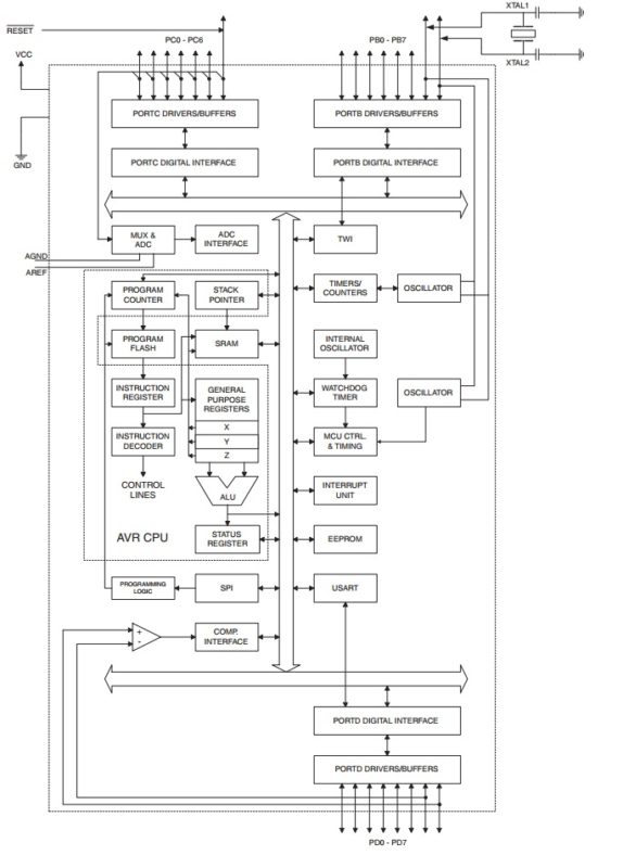
The ATmega8 provides 8 Kbytes of In-System Programmable Flash with Read-While-Write capabilities, 512 bytes of EEPROM, 1 Kbyte of SRAM, 23 general purpose I/O lines, 32 general purpose working registers, three flexible Timer/Counters with compare modes, internal and external interrupts, a serial programmable USART, a byte oriented two wire serial interface, a 6-channel ADC (eight channels in TQFP and QFN/MLF packages) with 10-bit accuracy, a programmable Watchdog Timer with Internal Oscillator, an SPI serial port, and five software selectable power saving modes.

Features
- Advanced RISC Architecture
- 130 Powerful Instructions – Most Single-clock Cycle Execution
- 32 × 8 General Purpose Working Registers
- Fully Static Operation
- Up to 16MIPS Throughput at 16MHz
- On-chip 2-cycle Multiplier
- High Endurance Non-volatile Memory segments
- 8Kbytes of In-System Self-Programmable Flash program memory
- 512Bytes EEPROM
- 1Kbyte Internal SRAM
- Write/Erase Cycles: 10,000 Flash/100,000 EEPROM
- Data retention: 20 years at 85°C/100 years at 25°C (1)
- Optional Boot Code Section with Independent Lock Bits
- In-System Programming by On-chip Boot Program
- True Read-While-Write Operation
- Programming Lock for Software Security
- Peripheral Features
- Two 8-bit Timer/Counters with Separate Prescaler, one Compare Mode
- One 16-bit Timer/Counter with Separate Prescaler, Compare Mode, and Capture Mode
- Real Time Counter with Separate Oscillator
- Three PWM Channels
- 8-channel ADC in TQFP and QFN/MLF package (Eight Channels 10-bit Accuracy)
- 6-channel ADC in PDIP package (Six Channels 10-bit Accuracy)
- Byte-oriented Two-wire Serial Interface
- Programmable Serial USART
- Master/Slave SPI Serial Interface
- Programmable Watchdog Timer with Separate On-chip Oscillator
- On-chip Analog Comparator
- Special Micro-controller Features
- Power-on Reset and Programmable Brown-out Detection
- Internal Calibrated RC Oscillator
- External and Internal Interrupt Sources
- Five Sleep Modes: Idle, ADC Noise Reduction, Power-save, Power-down, and Standby
- I/O and Packages
- 23 Programmable I/O Lines
- 28-lead PDIP, 32-lead TQFP, and 32-pad QFN/MLF
- Operating Voltages
- 2.7V – 5.5V (ATmega8L)
- 4.5V – 5.5V (ATmega8)
- Speed Grades
- 0 – 8MHz (ATmega8L)
- 0 – 16MHz (ATmega8)
- Power Consumption at 4Mhz, 3V, 25C
- Active: 3.6mA
- Idle Mode: 1.0mA
- Power-down Mode: 0.5µA
Let’s look at the ATmega8 pin diagram in detail.
ATmega8 Pin diagram and description
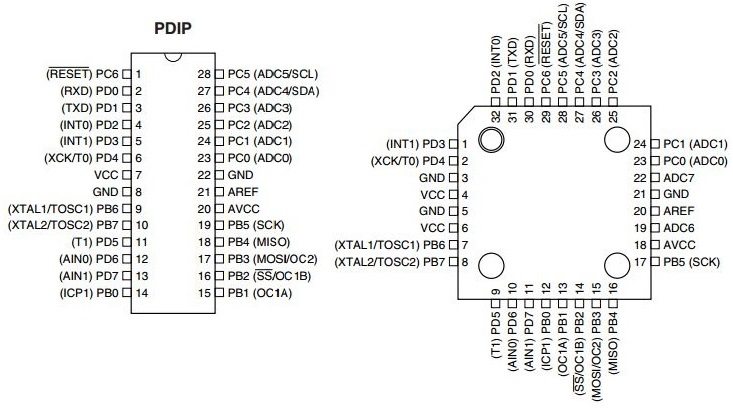
Detailed description of the ATmega8 pin diagram:
VCC: Digital supply voltage.
GND: Ground.
Port B (PB7…PB0) XTAL1/XTAL2/TOSC1/TOSC2
Port B is an 8-bit bi-directional I/O port with internal pull-up resistors (selected for each bit). The Port B output buffers have symmetrical drive characteristics with both high sink and source capability. As inputs, Port B pins that are externally pulled low will source current if the pull-up resistors are activated. The Port B pins are tri-stated when a reset condition becomes active, even if the clock is not running.
Port C (PC5…PC0)
Port C is a 7-bit bi-directional I/O port with internal pull-up resistors (selected for each bit). The Port C output buffers have symmetrical drive characteristics with both high sink and source capability. As inputs, Port C pins that are externally pulled low will source current if the pull-up resistors are activated. The Port C pins are tri-stated when a reset condition becomes active, even if the clock is not running.
PC6/RESET
If the RSTDISBL Fuse is programmed, PC6 is used as an I/O pin. Note that the electrical characteristics of PC6 differ from those of the other pins of Port C.
If the RSTDISBL Fuse is unprogrammed, PC6 is used as a Reset input. A low level on this pin for longer than the minimum pulse length will generate a Reset, even if the clock is not running.
Port D (PD7…PD0)
Port D is an 8-bit bi-directional I/O port with internal pull-up resistors (selected for each bit). The Port D output buffers have symmetrical drive characteristics with both high sink and source capability. As inputs, Port D pins that are externally pulled low will source current if the pull-up resistors are activated. The Port D pins are tri-stated when a reset condition becomes active, even if the clock is not running.
RESET
Reset input. A low level on this pin for longer than the minimum pulse length will generate a reset, even if the clock is not running. Shorter pulses are not guaranteed to generate a reset.
Vcc
Vcc is the supply voltage pin for the A/D Converter, Port C (3…0), and ADC (7…6). It should be externally connected to Vcc, even if the ADC is not used. If the ADC is used, it should be connected to Vcc through a low-pass filter. Note that Port C (5…4) use digital supply voltage, Vcc.
ARef
ARef is the analog reference pin for the A/D Converter. ADC7…6 (TQFP and QFN/MLF Package Only) In the TQFP and QFN/MLF package, ADC7…6 serve as analog inputs to the A/D converter. These pins are powered from the analog supply and serve as 10-bit ADC channels.
ATmega8 Microcontroller Sleep Modes
The idle mode stops the CPU while allowing the SRAM, timer/counters, SPI port, and interrupt system to continue functioning. The power down mode saves the register contents but freezes the oscillator, disabling all other chip functions until the next interrupt or hardware reset. In power-save mode, the asynchronous timer continues to run, allowing the user to maintain a timer base while the rest of the device is sleeping. The ADC Noise reduction mode stops the CPU and all I/O modules except asynchronous timer and ADC, to minimize switching noise during ADC conversions. In standby mode, the crystal/resonator oscillator is running while the rest of the device is sleeping. This allows fast start-up combined with low-power consumption.
The microcontroller operates in 5 sleep modes.
Power save Mode: It is used when Counter/Timer is clocked asynchronously. In general this mode used for saving the operational power requirement of microcontroller.
Idle Mode: It stops the functioning of CPU, but allows operation of ADC, TWI, SPI, and interrupts system and Watchdog. It is achieved by setting SM0 to SM2 bits of Microcontroller Unit register flag at zero.
Power down Mode: It enables external interrupts, the 2-wire serial interface, and watchdog while disabling the external oscillator. It stops all generated clocks.
ADC Noise Reduction Mode: It stops the central processing unit but allows the functioning of ADC, timer/counter and external interrupts.
Stand By mode: In this mode, only oscillator can operate by slowing all other operation of microcontroller.
Detailed datasheet available here.
More basic articles available in the learning corner.
