
N channel Enhancement MOSFET is a 3-terminal device. Let us first take a look at its construction followed by the working principle and VI characteristics.
Also Read: MOSFET Basics

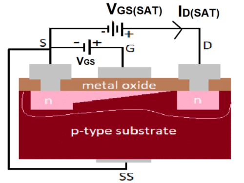
The body of any N-channel MOSFET is made up of P-type material. 2 N-type materials are diffused at the top. A depletion region will be formed in the PN junction. A metal contact is made at the bottom of the P-type substrate and a terminal is taken out called the body or substrate.
Similarly, a metal contact is made at the top of both the N-type materials, and two terminals are taken out as Drain and source. A Silicon dioxide layer is drawn in between the two N-type wells at the top. A metal contact is made at the top of it and a terminal is taken out called a Gate terminal. You can see it is a 4-terminal device. But we earlier said that it is a 3-terminal device.
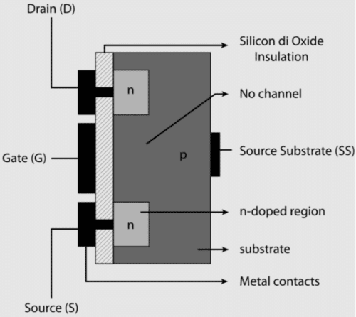
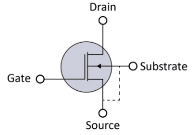
Now, what happens is generally the body terminal and source terminal are internally shorted and connected to the ground. Hence now only three terminals are visible namely Source, Drain, and Gate.
The Enhancement type of MOSFET does not have any channel present. So how will the current flow? To understand this we will move on to the working principle of N-channel Enhancement type MOSFET.
N-Channel Enhancement MOSFET Working
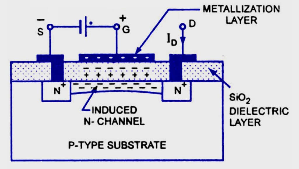
To get the drain current first we have to create a channel for the free movement of electrons. To create a channel we have to apply a voltage between the gate and the source terminal keeping the Gate at a higher potential. This voltage is called VGS. Now the gate is at higher potential. The free electrons will move toward the gate terminal. As discussed earlier we have a Silicon Dioxide layer at the top. Hence these free electrons will accumulate near the Gate region and will not escape. The silicon dioxide layer also acts as a dielectric. It will allow more free electrons to accumulate near the gate terminal in less applied voltage at the gate terminal.
Now on increasing VGS further, a high electric field is developed forcing atoms inside the P substrate to break. The free electrons generated will fill the holes near the gate region. This way holes are pushed away from the gate terminal increasing N-type behavior near the gate terminal. A time will come when an N-channel is created between the two N wells. The VGS voltage at which the channel is created is called the threshold voltage or VT. We can conclude from this discussion when VGS > VT an N channel is induced near the gate terminal as shown in the figure below.
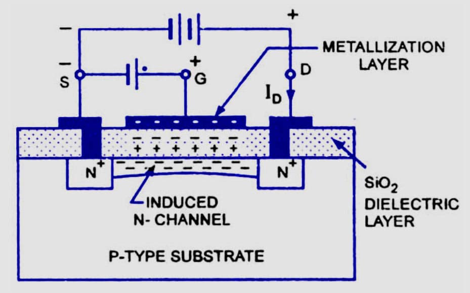
A channel is created still we are not getting any current. Let us see how to get the drain current. Apply a voltage source between the drain and the source keeping the drain at a higher potential. This voltage is called VDS. On applying this voltage current will start flowing from drain to source. This current is called drain current or ID.
We can conclude from this discussion, when VGS > VT and VDS > 0, the current ID flows from drain to source as shown in the figure below.
On increasing VDS further ID will increase. But will this ID keep on increasing with the increasing value of VDS? The answer to this question is no.
On increasing the positive voltage at the drain terminal a reverse bias is formed at the PN junction near the drain terminal. This will result in a thick depletion region near the PN junction. Hence on increasing VDS further, you will see the channel near the drain terminal is becoming narrow. The drain current will face more resistance near the drain terminal. A situation will reach when the drain current becomes constant and will not increase further.
This situation is called the pinch-off situation and the drain current is called the saturation current. The voltage at which we will get saturation current is called saturation voltage. We can conclude from this discussion, that pinch-off is reached when VGS > 0 (constant) and VDS = VDS(SAT), ID = ID(SAT) as shown in the figure below.
Now is there any way to increase the drain current beyond saturation? The answer is yes. Increasing ID further increases the value of VGS. This will increase the width of the complete N-channel. Hence VGS is controlling voltage.
N-channel Enhancement MOSFET V-I Characteristic
Now we can plot VI characteristics very easily. In the VI characteristics, you will see the plots of VDS vs ID for various values of VGS.
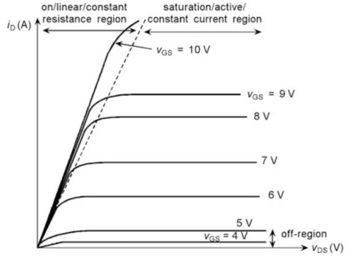
From the graph, it is clear that the current ID will become constant at a specific value of VDS. current ID increases only when the value of VGS is increased.