


P channel depletion MOSFET is a 3-terminal device similar to P channel enhancement MOSFET. The only difference between the two is the existence of a P-channel. In P channel depletion MOSFET, P-channel is already present. All other things are the same, as you can see in the figure below.
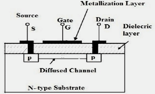
P channel depletion MOSFET is similar to N channel enhancement depletion, the only difference is in the polarities of applied voltages.
Also Read: Different Types of MOSFET
Let us move on to the working of P channel depletion MOSFET followed by the VI characteristics. Since the channel is already present, unlike the enhancement type MOSFET, you also will get drain current at zero gate voltage.
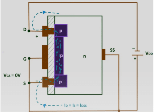
In our first case, let us connect the Gate terminal to the ground and apply a negative voltage at the drain and source.
On applying negative VDS, the holes in the P channel will move towards the negative drain terminal, and the drain current or ID will start flowing. On increasing the negative value of VDS further, keeping VGS at 0, a time will come where ID will become constant, and that value of drain current is called saturation current.
We can conclude from this discussion that when VGS = 0 and VDS < 0, current ID flows from and on increasing the negative value of VDS further, ID = IS = IDSS, as shown in the figure below.
Now let us see the effect of gate voltage on P channel depletion MOSFET.
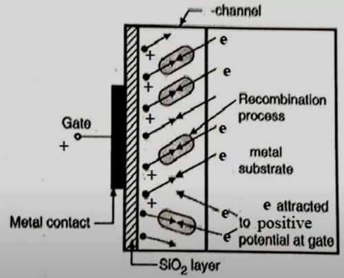
Apply VGS > 0. Electrons from the N-type substrate will attract towards the positive gate terminal and recombine with holes in the P channel, forming electron-hole pairs. On increasing positive potential at the gate, more electron-hole combinations will occur, decreasing the number of free holes in the P channel.
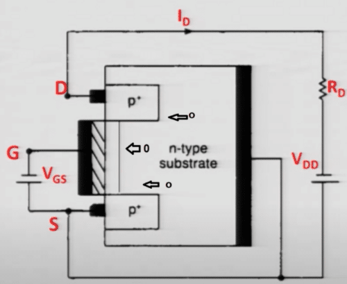
As a result, ID decreases. A time will come when the drain current will become zero. The positive gate voltage at which the drain current is zero is called pinch-off voltage or VP.
We can conclude from this discussion at pinch-off, VGS = VP, VDS < 0, and ID = 0, as shown in the figure below.
Now we will see the effect of negative gate voltage on the drain current.
On applying VGS < 0, the minority carriers in the N-type substrate, i.e. holes, will attract towards the gate terminal, thereby increasing the concentration of holes in the P-channel. As a result, the drain current will increase and exceed the saturation current.
We can conclude from this discussion, when VGS < 0 and VDS < 0, then ID > IDSS, as shown in the figure below.
As discussed earlier, depletion-type MOSFET worked for both positive and negative gate voltages. Now we can plot VI characteristics very easily. In the VI characteristics, you will see the plots of |VDS| vs |ID| for various values of VGS.
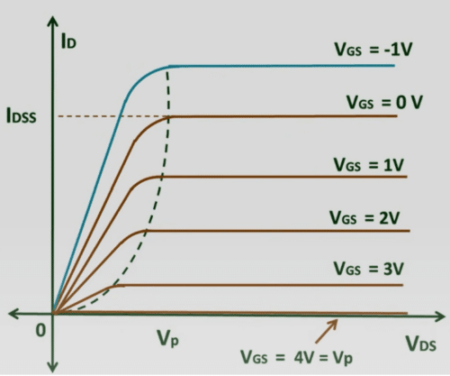
The graph shows that the current ID will flow for both positive and negative values of VGS. You can see from the graph that the drain current is less than the saturation current for the positive value of gate voltage, whereas, for the negative value of gate voltage, the drain current exceeds the saturation current. VGS = VP is also represented in this graph for which drain current is zero irrespective of drain to source voltage.

I’d love to try some depletion mode P channel FETs but I only seem to find articles that speak of them in theory, rather than by part number. Can someone recommend a common example of one that I can order?
Hello Mosquito,
You can order a variety of common P-channel Field-Effect Transistors (FETs) from electronic component distributors such as Digi-Key, Mouser, RS Components, or Arrow Electronics. Some popular P-channel FETs include:
1. IRF9540N: A widely used P-channel MOSFET with a maximum VDS of -100V and a maximum continuous drain current of -23A.
2. FQP27P06: A P-channel MOSFET with a maximum VDS of -60V and a maximum continuous drain current of -27A.
3. BS250: A small-signal P-channel MOSFET with a maximum VDS of -45V and a maximum continuous drain current of -230mA, suitable for low-power applications.
4. Si2301CDS: A P-channel MOSFET in a small SOT-23 package with a maximum VDS of -20V and a maximum continuous drain current of -2.3A.
5. Si2333CDS: Another small SOT-23 P-channel MOSFET with a maximum VDS of -30V and a maximum continuous drain current of -2.5A.
6. IRF4905: A P-channel MOSFET with a maximum VDS of -55V and a maximum continuous drain current of -74A, suitable for high-power applications.
7. FDG6321C: A dual P-channel MOSFET in a small SC-70 package with a maximum VDS of -20V and a maximum continuous drain current of -300mA.
When choosing a P-channel FET, consider your application’s voltage, current, and power requirements, as well as the package size that fits your design. Always check the manufacturer’s datasheet for detailed specifications and ensure the component meets your needs.