
Despite the wide-scale use of conventional CMOS detectors, a possibility exists for the development of image sensors that offer enhanced capabilities regarding increased temporal resolution, better dynamic range, reduced influence of scattering, and more.
Conventional image sensors are well-established. And it is expected that in future these will be upgraded with new sensor technologies that will allow us to acquire image based data having more details. This change is mainly influenced by the growing adoption of machine learning for which complex image analysis needs to be performed by computational algorithms. So, the question arises, what will the new image sensing technologies offer?
The answer to this question lies in the following points:
- Existing technologies, especially indium-gallium-arsenide (InGaAs) alloy for short-wave infrared (SWIR), are quite expensive and restricted to niche applications. To integrate them into an autonomous vehicle system, the costs need to be considerably brought down, which the new image sensors promise.
- The availability of increased computer processing power will require more accurate data for analysis and correlation. This is again possible with future high-end image sensors.
On a related note, more advanced sensors working together will surely improve object classification. By comparing the outputs from different sensor types, one will receive accurate insights. Take for example an advanced driver-assistance systems (ADAS) vehicle, which requires lidar, radar, and IR cameras for emergency braking, blind-spot detection, surround view, parking assistance, and much more. Besides this, the advanced sensors’ other applications include agriculture, land surveying, industrial monitoring, medical imaging, etc.
So, let’s take a look at these emerging image sensor technologies and the specific benefit each delivers.
SWIR image sensing
SWIR is an infrared technology whose wavelength range is 1,000nm to 2,000nm. It can only be detected by InGaAs sensors. In comparison, silicon CMOS image sensors are capable of detecting wavelengths of 400nm to 1,000nm (consisting of visible + near-infrared).
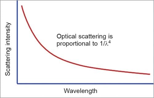
A key benefit of the SWIR image sensor is that it successfully helps in reducing light scatter.
From the graph in Fig. 1, we can deduce that scattering declines as the wavelength of light increases. This is beneficial for autonomous vehicles, ADAS systems, and drones.
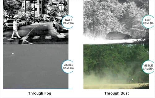
The image in the left side of Fig. 2 depicts a person walking through a road on a foggy day from the perspectives of a visible camera and a SWIR camera. A similar comparison has been made in the right side, which shows a car travelling through dust. These examples show the differences of an improved image range due to reduced scattering. SWIR also has many industrial applications for inspection purposes.
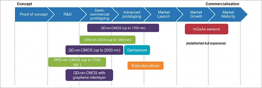
Options that will make SWIR technology feasible while replacing the incumbent InGaAs technology include:
- Extended Silicon. Absorption spectrum can be increased by shaping silicon
- Germanium
- Quantum Dots (QD)-on-CMOS. By changing the diameter of the dots, the wavelength size for absorption can be changed
- Organic-on-CMOS
Thin-film flexible photodetectors
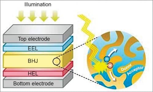
These can be considered to be solar cells that operate under reverse bias rather than forward bias.
An organic photodetector (OPD) consists of an electrode, wherein the bulk heterojunction (BHJ) is sandwiched between the electron extraction layer (EEL) and hole extraction layer (HEL). When illumination falls on the top electrode, the excited electrons travel to the BHJ to combine with the holes, producing a signal.
The advantage of thin-film photodetector over a silicon detector is that it can be flexible and printable. Since this type is suitable for covering large areas, applications could be biometric imaging (fingerprint detection), thin pulse oximeter, touchless control, and position and object detection.
Similar to the organic photodetectors, perovskite thin-film photodetectors use simpler/cheaper light-absorbing materials that can produce low-dark currents for increased detectivity or dynamic range and thus give more contrast to images.
Hyperspectral imaging
Although a bit established due to the use of conventional sensors, this technology has applications that are linked to emerging SWIR sensors. Hyperspectral imaging can be used outside the visible spectrum.
The basics of hyperspectral imaging technology lie in the availability of the entire spectrum wavelength at every pixel. So, while in a conventional image each pixel has red, green, and blue values, in hyperspectral imaging an entire spectrum is present. This can be achieved through point scan, line scan, wavelength scan, and snapshot, with each having a high spectral resolution.
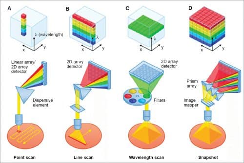
The line scan approach is very well suited for industrial imaging or land scanning via drones. The snapshot has been recently commercialised and is used in astronomy.
Other applications of hyperspectral imaging include:
- Agriculture
- Infrastructure
- Oceanography
- Surveying and extraction
- Chemical identification
- Identification of food degradation products
- Environmental monitoring
- Defence