
With higher efficiency and lower costs, perovskite–silicon tandem cells mark a breakthrough in solar tech. But with promise comes challenge. Can they truly help combat climate change?
Environmental pollution is sounding humanity’s death knell through climate change and biodiversity loss. As record-breaking summers, rising sea levels, and hazardous AQI levels threaten survival, the urgency to act is undeniable. The fight begins with a single step: carbon neutrality. Reducing fossil fuel use, expanding reforestation, and adopting renewable energy—solar, wind, hydroelectric, and geothermal—are critical tools in this battle.

Fortunately, renewable energy is gaining ground, steadily replacing fossil fuels and cutting greenhouse gas emissions. As of 2022, fossil fuels still account for 61 per cent of global energy, while renewables supply 29 per cent. Among these, solar leads the transition—now 90 per cent cheaper than a decade ago, driven by falling material and installation costs.
The International Renewable Energy Agency forecasts that by 2050, renewables could power 90 per cent of global energy demand, with solar capacity projected to soar from 1,200GW in 2022 to 75,000GW.
Sunlight to electricity; the science behind solar cells
Solar cells convert sunlight into clean, limitless energy—redefining how the world is powered. When sunlight hits a cell, the photovoltaic (PV) material absorbs it, generating electrical charges that flow as current.
Most solar cells today are first- or second-generation, made from silicon (Si), gallium arsenide, gallium indium phosphide, or cadmium telluride, with efficiencies ranging from 10 to 22 per cent. First-generation cells, primarily silicon-based, use P-type and N-type semiconductors created through doping.
Third-generation cells—based on emerging technologies like perovskites, dye-sensitised, and multi-junction designs—aim for efficiencies up to 40 per cent, exceeding the Shockley–Queisser limit of 30 per cent. Advances driving these gains include precise PV layer engineering, stability-enhancing additives, reduced optical losses, and grain optimisation.
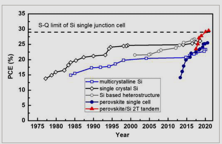
Laboratory-certified efficiency records include: multi-crystalline Si (23.3 per cent), single crystalline Si (26.1 per cent), heterostructure Si (26.7 per cent), perovskite single cells (25.5 per cent), and perovskite/Si 2T tandem cells (29.5 per cent), as shown in Fig. 2.
Why perovskites could revolutionise solar cells
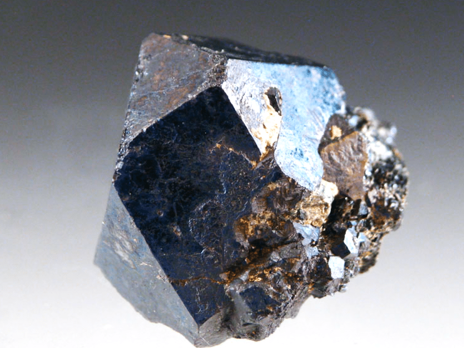
Perovskites are promising candidates for next-generation solar cells, thanks to their low cost, light weight, high efficiency, and ease of manufacturing. First discovered in 1839 by Russian mineralogist Lev Perovski in the Ural Mountains, the mineral—comprising calcium titanate oxide (CaTiO₃)—was named in his honour.
Today, ‘perovskite’ refers broadly to any octahedral ceramic oxide with the formula ABO₃, where ‘A’ is an alkaline earth or lanthanide metal cation, and ‘B’ is a transition metal anion.
Perovskites exhibit remarkable properties such as ferroelectricity, charge ordering, spin-dependent transport, and high thermopower. Their structure offers superior sunlight absorption compared to silicon, while their compositional flexibility enables precise tuning of optical and electrical properties.
High-efficiency perovskite solar cells (PSCs) typically follow the ABX₃ formula, where ‘A’ is a monovalent cation (e.g., methylammonium CH₃NH₃⁺, formamidinium CH₂(NH₂)₂⁺, Cs⁺, or Rb⁺), ‘B’ is a larger inorganic cation (such as Pb²⁺ or Sn²⁺), and ‘X’ is a halogen anion (iodine or bromine). These cells exceed 22 per cent power conversion efficiency (PCE) using 1,000 times less light-harvesting material than silicon.
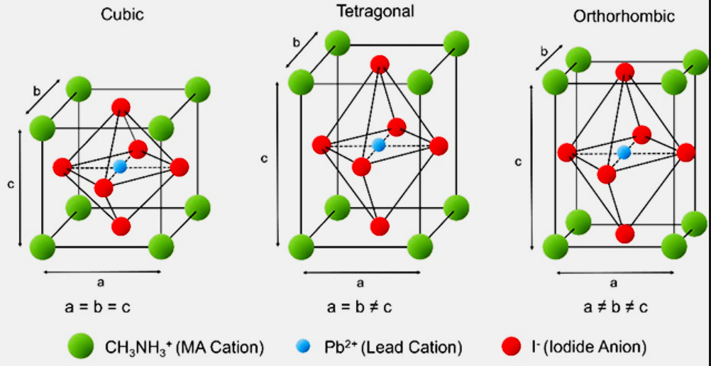
The cubic unit cell of 3D hybrid organometallic halide perovskites used in high-efficiency solar cells follows the ABX₃ structure: ‘A’ monovalent cations such as methylammonium (MA) occupy the cube corners, ‘B’ inorganic cations like Pb²⁺ sit at the body centre, and ‘X’ halogen anions (e.g., iodine) are positioned on the faces. MAPbX₃-based hybrid halide perovskites—an emerging class of low-cost solar materials—exhibit multiple phases depending on composition and temperature. In the beta phase, they offer improved absorption and stability, making them ideal for photovoltaic applications.
These materials exhibit high electron mobility (~800 cm²/V·s), long carrier diffusion lengths (>1 µm), and a strong absorption coefficient (10⁵ cm⁻¹), attributed to s–p antibonding coupling. Their low exciton binding energy (<10 meV) allows photogenerated carriers to behave as free electrons and holes, ensuring efficient charge transport.
Perovskites also feature a tunable bandgap (1.47–2.5 eV), modifiable through compositional engineering, nanostructuring, and quantum confinement—defining the minimum energy needed to excite an electron into the conduction band. The perovskite lattice accommodates element substitution within the Goldschmidt tolerance factor, further enhancing efficiency. A key advantage is their high open-circuit voltage (~1.3 V), significantly exceeding silicon’s 0.764 V, which reduces carrier recombination and improves overall performance.
Perovskite solar cells (PSCs) outperform conventional PV devices due to their broad absorption spectrum—from visible light (380–700 nm) to near-infrared (up to 800 nm)—maximising solar energy capture. They also offer flexibility, semi-transparency, lightweight construction, and customisable form factors. However, challenges persist: short operational lifespans, moisture-induced degradation, dependence on precious metals like gold and silver for electrodes, and the presence of toxic lead. Active research continues to address these limitations.
Steps to overcome hurdles
Perovskite solar cells (PSCs) reach efficiencies up to 25.2 per cent, exceeding silicon’s 20–22 per cent. This is achieved by bonding a treated tin dioxide (SnO₂) layer as an electron transport layer (ETL), reducing energy loss.
PSCs offer low-cost production, using solution or vapor deposition below 200°C—far less than silicon’s 1000°C. Ultra-thin perovskite layers efficiently capture sunlight while being lighter than silicon.
An intermediate tin oxide layer prevents electron–hole recombination at the junction, ensuring smooth charge transfer. Stabilising additives enhance durability without sacrificing light absorption, enabling open-circuit voltages up to 97 per cent of the theoretical maximum.
Lead content remains a concern, but encapsulation cuts lead leakage by 90 per cent. Noble metal electrodes and transparent substrates add cost, though recycling offers sustainability.
Ongoing improvements in efficiency, stability, and sustainability position PSCs to revolutionise solar energy as a cleaner, more affordable alternative to silicon panels.
The perfect bandgap combination
Each photovoltaic absorber converts only a specific sunlight range into electricity; other wavelengths go unused due to its bandgap. Thus, single-material solar cells top out near 30% efficiency. Silicon cells, for example, lose energy as heat through thermalisation when high-energy photons relax to the band edge.
This limit is overcome by stacking materials with different bandgaps in tandem. The top cell, with a larger bandgap, absorbs short wavelengths (UV, blue), while the bottom cell captures longer wavelengths (red, infrared), as shown in Fig. 5. This broadens absorption, reduces thermalisation loss, and boosts efficiency.
Perovskite cells efficiently convert visible light (380–700 nm), while silicon captures longer wavelengths. A perovskite layer atop silicon absorbs shorter wavelengths, letting infrared (800–2500 nm) reach the silicon layer. This tandem design raises efficiency beyond 30%, potentially over 40%, versus ~20% for silicon alone.
Fig. 5 categorises tandem cells into monolithic two-terminal (2T) and mechanical four-terminal (4T) configurations.
2T tandem solar cells
The sub-cells are connected in series via conductive layers, allowing the device to function as a single-junction solar cell, simplifying PV system integration. However, material choices are limited by the need for current matching, lattice compatibility, and suitable recombination layers or tunnelling junctions.
4T tandem solar cells
The two sub-cells are stacked vertically but operate independently at their respective maximum power points. This configuration eliminates current-matching constraints and does not require a conductive interlayer, but it increases module costs and power losses at larger scales. Due to fabrication complexity and higher costs, 4T tandem cells are less popular.
A third spectrally split design uses a spectral filter to direct 380–800nm light to the perovskite cell and 800–2500nm light to the silicon cell. This configuration offers flexibility in material selection but is costly due to the spectral filter.
For optimal performance, the bandgaps of the top and bottom cells must be carefully selected, as efficiency depends on their combination. The bandgap is the minimum energy required to excite an electron into conduction. In a two-junction tandem, a silicon bottom cell (1.1eV) paired with a perovskite top cell (1.62eV) achieves a theoretical efficiency limit of 42.4 per cent.
Beyond perovskite/silicon tandems, perovskite/CIGS (copper indium gallium selenide) tandems also show promise. Notably, perovskite/CIGS TSCs retain 85 per cent of their initial efficiency even after 68MeV proton irradiation, whereas perovskite/Si TSCs retain only 1 per cent due to increased recombination centres. However, perovskite/CIGS tandems face challenges such as lower efficiency, limited market presence, and difficulty integrating perovskite onto the rough CIGS surface.
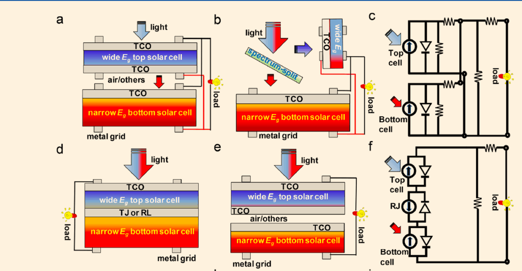
Key for Fig. 5:
- (a) – 4T Tandem Solar Cell (TSC) without spectrum split
- (b) – 4T Tandem Solar Cell (TSC) with spectrum split
- (c) – Equivalent circuit of a 4T TSC
- (d, e) – Scheme of a 2T Tandem Solar Cell (TSC)
- (f) – Equivalent circuit of a 2T TSC
Architecture of a perovskite/Si tandem cell
A simplified schematic arrangement of perovskite/Si tandem solar cells is shown in Fig.6.
Metal halide perovskites have recently made outstanding development to reach efficiency beyond 25 per cent. They can now be made using cost-effective technology. They have a high bandgap that is tunable. Si solar cells dominate the market, and their price is quite affordable. Their efficiencies have reached up to 25.6 per cent, already very close to the theoretical limit. So the most logical route to have a system with ultra-high efficiency is to use perovskite and silicon cells in tandem configuration to get the best out of them. In such a tandem device, the perovskite cell acts as the top cell, absorbing the visible light, and the silicon cell,l with a narrow band gap harvesting photons from the near-infrared part of the solar spectrum, acts as the bottom cell. Perovskite with pyramid textures and fullerene layers in 2T tandem configuration and silicon has propelled the new device to achieve 33.7 per cent efficiency very recently.
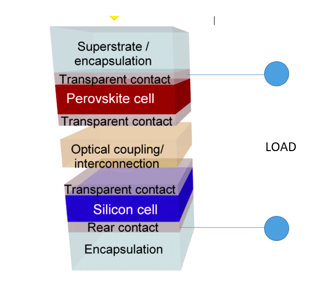
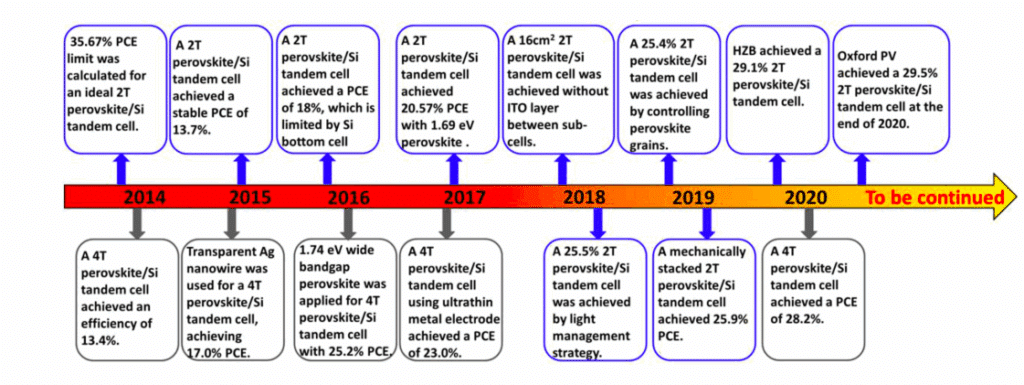
Fig. 7, shows the chronology of progress of increasing PCE of perovskite/Si TSC. It depicts how continuous research work has increased the efficiency from 13.4 per cent in 2014 to 29.5 per cent in 2020.
The PSCs can be classified based on the direction of charge carrier collection into two types: n-i-p (normal) and p-i-n (inverted). It is designated by stacking order of the charge transport layer (CTL) and the perovskite from the substrate, as shown in Fig.8.
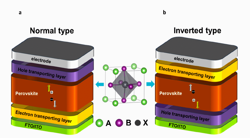
High-efficiency perovskite/silicon tandem solar cells often use p-i-n type PSCs due to their stability, low-temperature processability, and multi-junction compatibility. In these devices, the perovskite layer is sandwiched between an electron transport layer (ETL) and a hole transport layer (HTL). Common ETLs include PCBM (an organic butyric acid methyl ester), while HTLs are often PTAA, PEDOT: PSS, or NiO. Performance can be impacted by factors like light propagation, interface energetic barriers and parasitic absorption. Ongoing research aims to develop non-fullerene n-type charge transport materials with optimal energy levels, low light absorption, and moisture resistance. Charge transport optimisation through dopants in perovskite layers is a key focus of current research.
Now, Fig. 11 shows the architecture of a tandem perovskite/Si solar cell, where a top p-i-n metal halide perovskite is combined with a rear junction silicon heterojunction bottom cell. This arrangement has achieved a certified PCE of 26 per cent, with the potential to reach 31 per cent PCE with optimisation of the thickness of active materials, grain engineering, and improving the design. Light enters the top perovskite cell, which consists of the following layers:
- Silver electrode:
- 200nm thick Ag layer formed by sputtering on aluminium zinc oxide (AZO) surface
- Good electrical conductor, facilitating electron movement
- LiF layer:
- 117nm thick, formed by thermal evaporation
- Acts as an interface layer to suppress perovskite decomposition
- Enhances SnO2 conductivity and energy band alignment
- Provides anti-reflection, increasing photo-generated current by 1.5mA/cm²
- IZO layer:
- Transparent top electrode, 117nm thick, composed of indium zinc oxide (IZO) (deposited by sputtering)
- High carrier mobility, low carrier concentration, suitable for transparent electrodes like ITO
- Optimised thickness minimises parasitic absorption and lowers sheet resistance
- Can be sputtered at 100°C, unlike ITO which requires 300°C, preventing damage to underlying layers
- SnO2 layer:
- Atomic layer deposition (ALD) coated tin oxide buffer layer
- Protects sensitive layers, including perovskite, during sputtering
- C60 layer:
- Fullerene (C60) acts as an electron transport layer (ETL) in p-i-n configuration
- Small conduction band offset, large valence band offset, favourable for electron extraction and hole-blocking
- High electron mobility, hydrophobic, and helps passivate perovskite antisite defects
- Perovskite:
- Absorbs visible light (380–700 nm) with “triple cation” composition (Cs0.05Fa0.8MA0.15Pb(I0.75Br0.25)3)
- Common recipe for tandem cells: Cs0.1(MA0.9)Pb(I0.9Br0.1)3, yielding ~26 per cent PCE
- PCE increases to ~31 per cent with pentafluorobenzylphosphonic acid treatment
- Bandgap tunable (1.1 eV to 3.0eV)
- Efficiency limited by Voc loss and halide phase segregation for wide bandgap PSCs
- Perovskite thickness (300–470nm) optimised for current matching (Jsc ~19.5 mA/cm², high PCE).
- Wide bandgap absorbers show little hysteresis and high stability (PCE > 27 per cent).
- Deposition methods: vacuum deposition and solution processing (higher efficiency)
- PTAA Layer (HTL):
- Polytrimethyl phenylamine (PTAA) is used as hole transport material (HTL)
- Excellent hole-transporting and electron-blocking properties
- Coated on perovskite surface via spin or nitrogen blade coating, annealed at 100°C for 10 minutes
- PTAA provides lower parasitic absorption losses
- ITO Layer:
- Functions as a recombination layer between sub-cells, ensuring current flow
- 20-40nm thick, deposited on nc-SiOx: H interlayer
- Transparent and electrically conductive, reducing optical losses and boosting electron-hole recombination
- Doped with ZnO nanoparticles for moisture protection, enhancing perovskite layer stability
- Acts as a charge current collecting electrode and protects the bottom cell during processing
Photo-generated carriers from one sub-cell recombine with opposite-charge carriers from the other in the interconnecting layers (ICL), ensuring efficient recombination, minimal VocV_{oc} loss, and high fill factor (FF) for improved PCE. Reducing parasitic absorption above 800 nm and optimising refractive index matching between perovskite and c-Si minimises optical losses affecting JscJ_{sc}. The tandem cell in Fig. 11 uses IZO (top) and ITO/AZO (bottom) interlayers, creating high index contrast. Increasing oxygen content in silicon reduces its refractive index, making hydrogenated nanocrystalline silicon oxide (nc-SiOx:H) an effective intermediate layer for bottom Si cells.
Silicon bottom cell layer structure
- nc-SiOx:H Layer (90 nm, n-doped)
- Acts as an electron and hole-selective stack
- Enhances conductivity and transparency by combining nc-Si:H with a-SiOx:H
- Improves light coupling into the Si bottom cell and reduces reflection
- Forms an electron-selective contact with a 20 nm ITO recombination layer
- Hydrogen at the a-Si: H/c-Si interface passivates defects, increasing PCE
- c-Si(n) Layer (260µm, n-type float zone Si)
- Low defect density, uniform crystal orientation, and high carrier lifetime
- Front surface polished; rear chemically textured with a pyramidal structure to reduce reflection
- Texturing decreases reflectance (from 30–40%) and improves light absorption
- Polished rear side facilitates perovskite and carrier-selective layer deposition
- New conformal deposition process enables both-side etching for improved light harvesting
- a-Si(i) Layers (5nm each, both sides of c-Si(n))
- Intrinsic hydrogenated amorphous silicon passivates the c-Si surface
- Reduces surface recombination velocity and improves carrier collection
- Transparent to the solar spectrum and effectively terminates Si dangling bonds
- a-Si(p) Layer (5nm, textured backside)
- P-doped a-Si:H forms the junction of the silicon heterojunction (SHJ) cell
- AZO Layer
- Aluminium-doped zinc oxide replaces ITO for bottom cell contact
- Ag Electrode (200 nm, sputtered on AZO)
- High electrical conductivity facilitates electron transport
Charge transport and recombination
- Photo-generated holes in the c-Si bottom cell move through the a-Si(p) layer to the AZO
- Electrons from the perovskite top cell pass through SnO₂ to the IZO layer
- Recombination occurs at the AZO layer, with ITO, AZO, or IZO as viable recombination layers.
Optimisation and performance
- IZO, SnO₂, and C₆₀ absorb in the UV; AZO and Ag absorb in the infrared
- Proper design minimises optical losses and enables:
- Jsc > 19.7mA per sub-cell, Jpero+si > 40mA cumulative
- Voc of 1.77V and reduced series resistance.
- PCE > 30 per cent for tandem perovskite/silicon solar cells
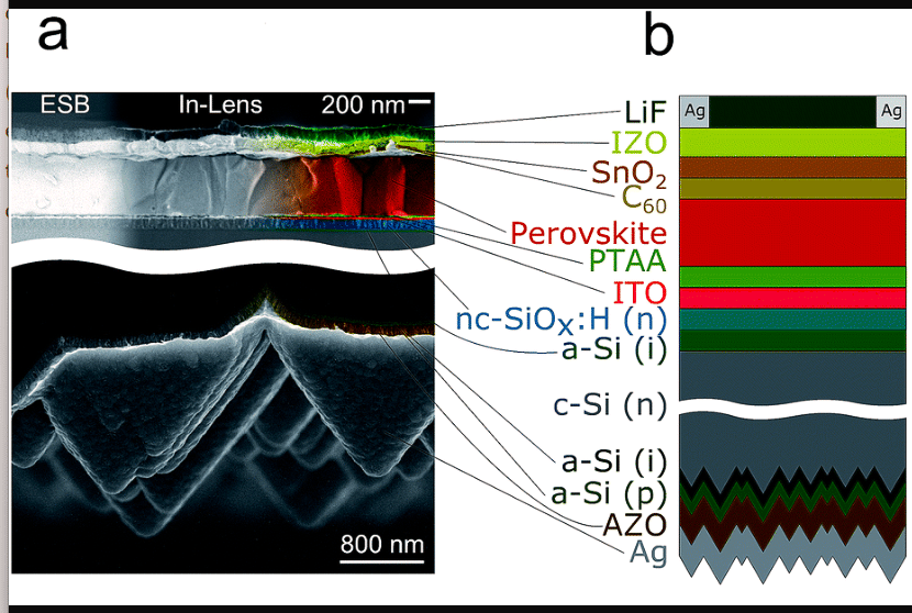
Key to Fig. 11
- a) – SEM image of the cross-section
- b ) – architecture of the perovskite/Si TSC
Cost analysis
Monolithic tandem perovskite/Si solar cells are commercially promising but face challenges in stability and material toxicity. Encapsulation is crucial to counteract degradation from humidity, thermal stress, and UV exposure. Improved composition engineering is needed to mitigate hysteresis, while scalable manufacturing and larger PSC sizes must be developed. Currently, their lifespan is three years, far from silicon’s 20-year durability. Continued R&D aims to enhance design, extend lifespan, and lower costs for mass production. Future tandem perovskite PVs are expected to achieve a 20-year lifespan, with cost estimates analysed using a bottom-up approach. The levelised cost of electricity (LCOE) of solar modules is used here to evaluate the techno-economic competitiveness of three types of modules, namely:
- Module A – composed of traditional c-silicon cells
- Module B – made from planar perovskite (PVSK) cells
- Module C – composed of c-silicon/perovskite tandem solar cells (TSC) with the architecture shown in Fig. 11.
- LCOE = Total levelised cost/total lifetime electricity production
Basis of cost analysis:
1. Production Capacity: 100MW per year for the solar cell plant.
2. Manufacturing cost includes the following components:
– Raw material cost
– Utilities
– Labour
– Equipment maintenance
– Depreciation (over five years)
3. Module lifespan: Assumed to be 20 years
4. Degradation rate: 1 per cent per year for all modules
| Description | Unit | c-Silicon | Planar PVSK | c-Si/PVSK Tandem |
| 1. PCE | per cent | 21 | 20.1 | 25 |
| 2. Cost of Manufacturing | $/m² | 89.6 | 32.7 | 121 |
| 3. Module Cost | $/W | 0.43 | 0.17 | 0.48 |
| 4. LCOE | US Cents/W | 5.50 | 4.34 | 5.22 |
Table 1. Cost analysis
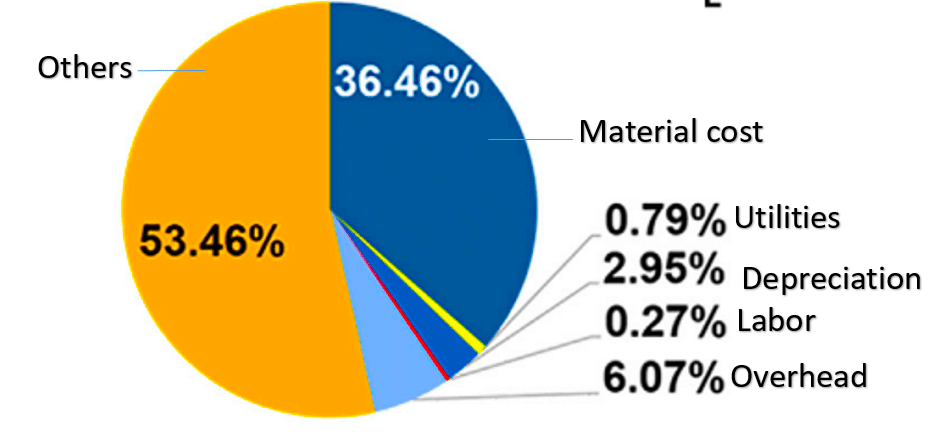
From the table above, it can be observed that although the cost of modules A and C per watt of electricity is nearly the same, the LCOE for the tandem cell (C) is 5 per cent lower than that for the c-Si (A) cell, due to the higher PCE of the tandem cell. Currently, researchers in laboratories have already achieved perovskite/Si tandem cells with a PCE of 31 per cent. Therefore, it is anticipated that the LCOE using tandem cells will be further reduced in the near future. A pie chart illustrating the various components of the cost for module C is shown in Fig. 12.
Manufacturing technique
Silicon solar cell fabrication
Monocrystalline silicon ingot wafers are cut, cleaned, and textured using a potassium hydroxide-based etchant in a pyramidal pattern. Intrinsic a-Si and p-type a-Si:H films are then deposited on both sides via plasma-enhanced chemical vapour deposition. A 20nm ITO layer is sputtered on the front, followed by an AZO layer on the rear, with a 200 nm silver layer subsequently sputtered onto the AZO. The silicon cells are annealed at 200°C for 20 minutes before perovskite cell fabrication. Finally, the silicon wafer is laser-scribed into 16mm × 16mm chips.
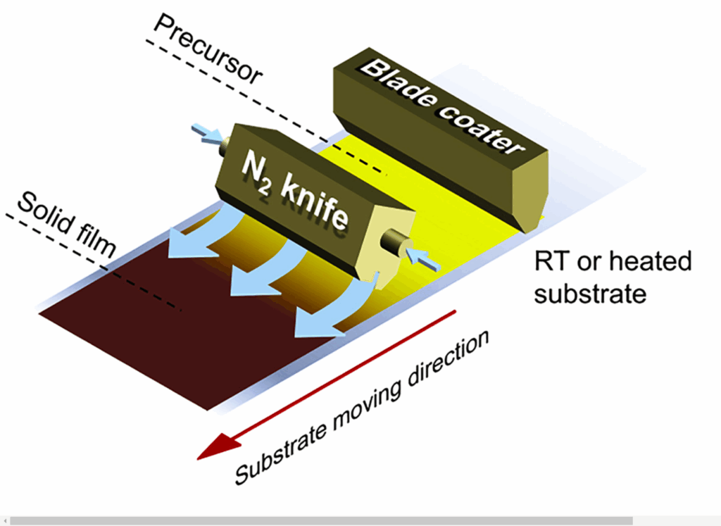
Perovskite/silicon tandem solar cell fabrication
Tandem architecture is achieved via nitrogen-assisted solution-based blading (Fig-13), enabling scalable deposition onto silicon wafers at 1.5 m/min. The PTAA hole transport layer is coated at 25 mm/s on the ITO layer of the Si bottom cell using a nitrogen knife at 50–70°C. A Cs₀.₁MA₀.₉Pb(I₀.₉Br₀.₁)₃ precursor is blade-coated at ambient conditions to form the perovskite active film, followed by thermal deposition of C₆₀ by evaporation and atomic layer deposition (ALD) of SnO₂ at 600°C. The top transparent electrode, IZO, is sputtered onto the SnO₂ layer. To minimise lateral transport loss, 200 nm-wide Ag fingers are sputtered onto the IZO layer.
Final thoughts
Since 2009, PSC efficiency has risen five-fold, making it ideal for tandem integration with silicon, capturing a broader solar spectrum with minimal heat loss. Researchers are further enhancing the stability and efficiency through different methods to improve its performance. Its three-decade-long lifespan will pave the way for a better, sustainable, carbon-neutral energy future.
Authored By: Rathindra Nath Biswas. The author, now retired, is the former head of MECON Limited (a PSU under the government of India), Durgapur, West Bengal.