


Explore circuits, design considerations, and IC marvels – empowering the future of energy solutions.
With the advent of new energy sources and the requirement for power supply in various forms and sizes, there will be a huge demand for new designs, with efficiency and reliability being paramount.

Through this topic, we will discuss various forms of power supply units in different forms. These are the critical roles through which power electronics will play its role in modern electronics design:
• Power generation
• Power transmission
• Power distribution
• Power control
However, the basic concept remains that in all these applications, the input voltages and currents are switched using power semiconductor devices to provide desired outputs.
Latest advancements in various switching semiconductors and easy availability have definitely made this market segment lucrative and, most importantly, affordable.
Through this discussion, we will concentrate on these 4 basic types of power electronic circuits:
1. AC input to DC output: Commonly known as SMPS or power supply in general
2. DC input to DC output: buck, boost, and CUK converters
3. DC input to AC output: UPS/Inverters
4. AC input to AC output: Voltage converters and isolators (commonly known as cyclo converters)
We shall concentrate on the first type of power supply design ideas in this discussion:
SMPS (Switched Mode Power Supply) is a complex yet affordable solution for modern power supply requirements. This unit will convert the line voltage to usable voltage/current using the high-frequency switching method. There are numerous approaches to achieve this, and each topology is explained below:
- Buck converter – Low voltage and medium current
- Boost converter – High voltage and low current
- Buck-Boost converter – Special applications
- SEPIC/Ćuk converter – Special applications
- Flyback converter – Considered when power requirement is below 100 watts and current is below 10 Amps (typically low voltage and low current):
- Single-switch flyback – Considered when power requirement is below 0 – 100 watts and current is below 10 Amps (typically low voltage and high current)
- 2-switch flyback – Considered when power requirement is below 0 – 400 watts and current is above 10 Amps (typically medium voltage and low current)
- Active clamp flyback – Considered when power requirement is below 0 – 100 watts and current is above 10 Amps (typically low to medium voltage and high current)
- Forward converter
- Push-Pull converter – Considered when power requirement is between 1000 – 4000 watts (typically medium voltage and high current)
- Half-Bridge converter – Considered when power requirement is between 0 – 400 watts and current is above 10 Amps (typically medium voltage and high current)
- Resonant LLC Converter
- Phase-shifted full bridge – Considered when power requirement is between 400 – 4000 watts
- Active clamp forward – Considered when power requirement is up to 400 watts and current is above 10 Amps (typically medium voltage and high current)
- 2-switch forward – Considered when power requirement is up to 100 watts and current is above 10 Amps (typically low to medium voltage and high current)
- Single switch forward – Considered when power requirement is below 0 – 100 watts and current is below 10 Amps (typically low voltage and high current)
- DCM flyback – Considered when power requirement is up to 100 watts and current is below 10 Amps (typically low voltage and medium current)
- DCM 2-switch flyback: Special Application
Let’s discuss each of the design considerations, SOIC (small outline integrated circuit) design calculations, and application-specific components to be used for each type. We shall discuss each topic in our upcoming series separately.
Buck Converter
Design Considerations
This topology is meant to be non-isolated (i.e., the output is connected directly to the source). These types of converters are typically used as step-down regulators, replacing conventional linear regulators. However, it is to be noted that these converters are comparatively complex in design, but the high output efficiency voids this drawback when the output voltage is low. Most solutions can be achieved with a single IC solution with very minimal external components.
SOIC Availability
There are numerous ICs specifically meant for this topology. Some of the ICs that we definitely cannot ignore are:
- LM2576 by Texas Instruments
- RT6200 by Richtek
- MPM3610 by Monolithic Power Systems
- SY8105ADC by Richtek
- TPS54302DDCR by Texas Instruments
- A4490 by Allegro Microsystems
- TPS65400 by Texas Instruments
- RT9992 by Richtek
- LTC3374 by Analog Devices
And the list goes on for other ICs. Here LM2576 plays a prominent role due to its availability and decent performance for most of the applications. So let’s discuss the circuit designing of this IC.
This is a SIMPLE SWITCHER® Power converter working at 150 kHz, 3.3 V, 5 V, 12 V, and adjustable output versions. The adjustable version output voltage range is 1.2 V to 37 V ±4% maximum over line and load conditions while still maintaining 73% efficiency.
Available in TO-220 and TO-263 packages, which makes it easy for novice designers as well. The LM2596 series operates at a switching frequency of 150 kHz, thus allowing smaller-sized filter components than what can be required with lower-frequency switching regulators.
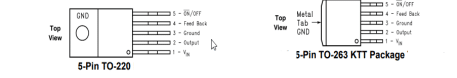
Pin Details
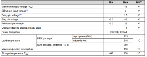
Absolute Maximum Ratings
Schematics
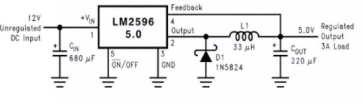
Schematics: Fixed voltage 3Amps load current.
The input voltage is fed to pin #1 (Vin). Input capacitor Cin is for ripple rejection and transient rejection. This capacitor must be placed close to the IC using short leads. A low ESR aluminium or tantalum bypass capacitor is required between the input pin and ground pin to prevent large voltage transients from appearing at the input.
It is worth noting that the RMS current rating of the input capacitor must be selected to be at least ½ the DC load current. It is advised to check the capacitor manufacturer’s datasheet for additional information about using this capacitor.
Pin #5 is used to shut down the voltage regulator circuit with the input supply current reducing to 80 uA. When the voltage on this pin goes below the threshold voltage of 1.3 V, it turns on the buck converter. And when the voltage goes above 1.3 V, it turns off the converter. This pin can be simply connected to GND to disable this feature.
Pin #4 is for the feedback loop to regulate the output voltage. This can be simply connected to the output voltage pin #2. It is always advised by designers to keep this line away from inductors in the vicinity which might induce stray flux into the feedback loop.
Pin #3 is for common GND, while pin #2 is for the output voltage, and it will be wise to consider a couple of components connected to this pin. Diode D1 is the catch diode, which should be at least 1.3 times greater than the maximum load current considering the losses.
This diode is carefully selected to be not stressful in extreme conditions like overload or short-circuit. 1N5823 Schottky diode will provide the best performance and will not be overstressed even for a short output.
Programming Output Voltage
Select R1 and R2.
VOUT = VREF (1 + R2/ R1) where VREF = 1.23 V
Inductor Selection (L1)
E*T = (VIN − VOUT − VSAT) (VOUT + VD)/ (VIN − VSAT + VD) (1000/ 150 kHz)
where,
VSAT = internal switch saturation voltage = 1.16 V
VD = diode forward voltage drop = 0.5 V
E = inductor volt
T= microsecond constant
Output capacitor selection (COUT)
In the majority of applications, low ESR electrolytic or solid tantalum capacitors between 82 μF and 820 μF provide the best results. This capacitor must be placed close to the IC using short capacitor leads and short copper traces. Do not use capacitors larger than 820 μF.
Feedforward capacitor (CFF):
For output voltages greater than approximately 10 V, an additional capacitor is required. The compensation capacitor is typically between 100 pF and 33 nF.
CFF = 1 /(31 *103 * R2)
This capacitor type can be ceramic, plastic, silver mica, and so forth
Tweaks
This is a tweaked circuit to vary the output voltage. At most caution to be exercised while using the feedback loop so that absolute max specs are not exceeded. POT R1 can be tuned to change the feedback voltage fed to the feedback pin, thus varying the output voltage without disturbing the voltage regulation.

