


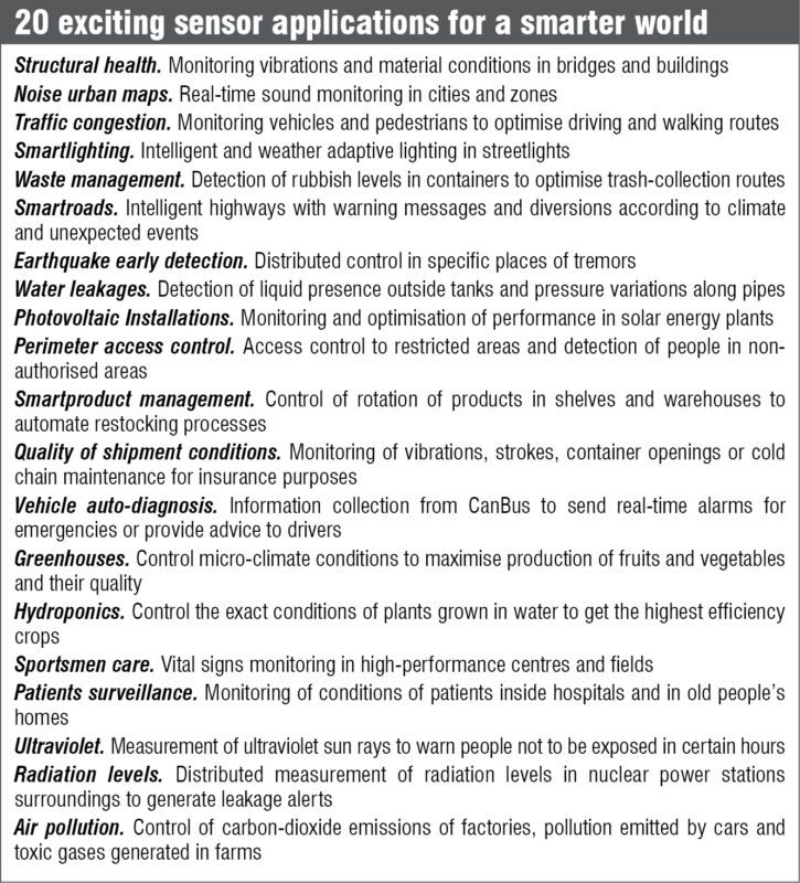
Sensors are everywhere; in your mobile phones, laptops, security devices and vehicles. Sensors like accelerometers, gyroscopes, temperature sensors, acoustic sensors and flow sensors that are already available in the market are (relatively) too large in size for some of the cutting-edge applications that are waiting for these.
“The sensors are available, but you need to miniaturise these a lot more. Instead of the Internet of Things (IoT), I would call it the Internet of Nanothings, because until you miniaturise the sensors and make these cost-effective, developers will not be able to utilise these,” said Dr Vijay Mishra, chief technology officer at Centre for Nano Science and Engineering (CeNSE) at Indian Institute of Science (IISc), Bengaluru, in a session delivered at India Electronics Week 2016.

Autarky in sensors
Autarky means economic independence or self-sufficiency. In sensor talk, energy autarkic sensors are those that can obtain energy needed from ambient temperature differences in the environment. Why? These temperature differences let the devices operate without batteries or wiring, thus enabling these to be self-sufficient little pieces of technology that can survive on their own.
Fraunhofer Institute of Physical Measurement (IPM) develops thermoelectric wireless sensors that can generate enough energy to supply various sensors, including their radio units, with enough energy to function properly. These can be used to implement wireless monitoring of body functions or to monitor material fatigue in aircraft.
The average German drinks about 150 litres of coffee per year, claims Fraunhofer IPM. Unsurprisingly, one of the popular innovations from energy-autarkic sensors led to the development of the communicating coffee pot. The pot uses heat from hot coffee to power the high-tech coffee pot’s sensor technology, which keeps a watch on coffee temperature and lets the kitchen team know if its coffee has gone cold. Ingenious, would you not say?
Wristbands and kits
Other examples of energy harvesting include BlueTEG sensor wristband that uses the temperature difference between the skin and the surrounding air to produce energy, and transmits data via Bluetooth. Sensors in applications to test structural integrity use piezoelectric collectors to gather energy from vibrational stresses.
One among the numerous solutions available is Wurth Electronics’ Energy Harvesting Solution To Go Kit, which helps developers apply these technologies in battery-less products. The kit can harvest energy through solar, electromagnetic, piezoelectric and thermal sources.
Sensing in biomedical
There are some interesting sensors developed at CeNSE such as Envirobat, a gas sensor. Others include pressure sensors ranging from those that can be used in the aeronautical industry that can measure 500 bars, to those meant for biomedical applications, which can measure a few millibars of pressure.
There is also a special biomedical pressure sensor that they have developed, which is implanted into the skull during neurosurgery. It continuously measures intracranial pressure, and is extremely useful when doctors are performing neurosurgery. This technology is readily available for people to commercialise.
Dr Mishra also talked about a solid-state gas sensor platform. The gas sensors contain a micro-heater that consumes only 13 to 14 milliwatts of energy. It is a power-efficient device and has a quick response time.
An electrode is deposited over the micro-heater. Over the electrode there is a sensing element that has a nano-structured film whose resistance changes when it is exposed to a particular gas. The film is made using carbon nano-particles, and is the key to the kind of sensitivity the device can have. Change in resistance is a function of concentration of gas.
Finally, a substrate layer is etched from the bottom. Thickness of the film is 13 to 14 microns. This is required so that the micro-heater does not take a long time to heat up. If the substrate layer is thick, a lot of heat gets dissipated, and the sensor uses more power. Once the device is ready, it is taken into a known ambient of that specific gas, and the sensor is tested.
High-tech health
An interesting device that has been fabricated at CeNSE lab and now has one United States patent and seven Indian patents is a diabetes sensor. Dr Navakanta Bhat has developed it to aid in diabetic management as well as to understand the long-term effects of diabetes on other organs of the body.
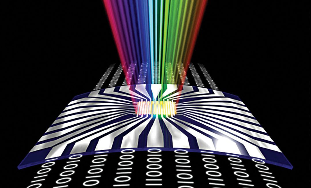
Ophthalmic OCT on a Chip (OCTCHIP) is a project started in 2016 that allows optical coherence tomography (OCT) systems to be built much cheaper through the use of photonic integrated circuits. The solution has a swept source, electrical interposer, photonic integrated circuit, micro-lens array and reference arm on a chip smaller than the new five-rupee coin. This project is funded by European Union’s Horizon 2020 research and innovation programme.
Wireless sensor networks
Wireless sensor nodes can be used to improve functionality and convenience of applications. Without wires to hinder installation, these sensors can be placed at strategic locations to continuously collect data on their surroundings. This makes these a perfect tool for building systems in line with the IoT concept where systems can autonomously collect data, process and actuate it in response to the information gleaned out of the data.
Fraunhofer has a technology called s-net that lets engineers create energy-saving wireless networks for long-lasting large-scale systems and smartobjects in an IoT network. Inside s-net, proprietary media-access protocol SlottedMAC combines the efficiency advantages of a time division multiple access system with scalability and flexibility of contention based protocols to enable an intermeshed networking of sensor nodes.
“Intermeshed networking creates the basis for accurate localisation of sensor nodes. Based on an enhanced weighted centroid localisation algorithm, the sensor node independently calculates its own position from the positions of all received nodes. As a result, the position is calculated in such a way that resources are spared, and this can be signalled to a central entity upon request or at set time periods. As the position is calculated directly on the node, applications can also trigger an alarm without network communication, for example, in the case of theft,” explains a paper on this technology.
Miniaturise
Sensor technology can be used to help miniaturise big laboratory equipment through advanced integration technologies.
Smaller labs. MICROMOLE project at Fraunhofer IIS is to reduce the size of a tabletop laboratory system down to an object that will fit in the hand, while being able to operate in wastewater without human intervention.
Main element of the system is the chemical sensor, which is miniaturised using micro-fluidic technology. It implements high sensitivity and selectivity, while being robust against variations in water properties due to a custom-designed sensitive electrode.
Pocket RADARs. One of the most exciting announcements made this year is Google’s Soli Project. It is a new sensing technology that uses miniature radar through an interaction sensor to detect touch-less gesture interactions. The sensor tracks sub-millimetre motion at high speeds with great accuracy.
The chip comes in an 8mm x 10mm package that emits electromagnetic waves in a broad beam and tracks the reflected beam for information. Soli sensor is a fully-integrated, low-power radar operating in 60GHz industrial, scientific and medical radio band. Infineon and Google will be jointly marketing this technology mid 2017 onwards.
Acti3D technology makes available algorithms for an optical sensor system that enables detection, localisation and analysis of movements without the output of real image data. Algorithms record important points and image features, independent of the ambient lighting. In a subsequent analysis, movements are classified and assigned to the foreground or background. This way, people can be distinguished from technical devices.
The future of sensing
There are quite some exciting and award-winning developments happening in this space, too. Bosch’s BMF055 won this year’s Innovation Award at Sensors Expo & Conference as the industry’s very first custom-programmable 9-axis motion sensor.
Another Innovation Award winner was AWAIBA’s NanEye 2D sensor, which is a system on chip with complementary metal-oxide-semiconductor image sensors.
Third in line was Siargo’s Fl1000 time-of-flight MEMS flow sensor.
With the strong growth of the IoT, research and development in sensor technology is already seeing quite some hectic activity. Let us hope it will get even more exciting in the coming year.
Dilin Anand is executive editor at EFY. He is B.Tech in ECE from University of Calicut, and MBA from Christ University, Bengaluru