




EDA is evolving from AI assistants to autonomous agents and collaborative intelligence. Here is what each wave means for semiconductor innovation.
Assessing the process from initial chip design to the final step of sending the design for manufacturing uncovers the operational challenges faced by design engineers, verification engineers, and project managers.
Most chip design activities are iterative and time-consuming, requiring repeated refinement. In addition, the verification stage often generates error logs with thousands of items that need to be addressed. Large semiconductor companies also manage extensive IP repositories, which are collections of reusable circuit designs and components. Some companies maintain libraries with over 50,000 items, including both in-house and third-party designs. Furthermore, multiple distributed teams often collaborate on a single chip design, causing delays as engineers wait for responses to their queries.

However, using both generative AI and traditional ML technologies can automate these processes to save time and improve semiconductor yield.
Artificial Intelligence (AI) and Machine Learning(ML) are playing an increasingly crucial role in optimising electronic design automation (EDA) across the semiconductor industry. This article explores the rising complexity and costs of designing chips at advanced nodes. It highlights how generative AI (GenAI) and deep reinforcement learning (DRL) help semiconductor companies accelerate time to market (TTM), improve yields, and lower costs over time. It also reviews how customising large language models (LLMs) with retrieval augmented generation (RAG) and fine-tuning significantly expands GenAI’s core capabilities for EDA processes and tasks.
Insights
- Artificial intelligence (AI) in semiconductor design enhances innovation, improves efficiency, and accelerates development, addressing the complexity and challenges in the ecosystem.
- Design accounts for over 53% of the semiconductor industry’s R&D expenses, highlighting its importance for the sector’s growth and innovation.
- Generative AI-driven solutions, such as automated IP search assistants, can improve productivity, reduce time-to-market, and optimise design processes.
- AI-powered floor planning and error log analysis improve design efficiency by automating complex tasks and reducing manual effort.
- The use of AI-driven tools like design copilots helps design engineers overcome collaboration challenges and streamlining communication and decision-making across teams.
The semiconductor industry is on track to become a trillion-dollar industry by 2030, fuelled by requirements for advanced chips in AI, 5G/6G communications, and data centres. While there is growth across the semiconductor value chain, a significant portion of value creation is driven by semiconductor design companies. Among the top 20 global semiconductor companies by market capitalisation, 13 are deeply engaged in chip design, including both fabless companies, which focus solely on design and outsource manufacturing — such as Nvidia, AMD, Qualcomm, and MediaTek — and design-led integrated device manufacturers (IDMs) like Intel, Samsung, Texas Instruments, and Analog Devices.
This dominance underscores how chip design remains the engine of innovation and market leadership in the industry. However, this central role has also brought growing challenges:
- The shift to advanced nodes (7nm and below) demands major design changes to handle increased circuit density and meet higher performance demands.
- Growing demand from AI and high-performance computing (HPC) leads to more complex chip designs, particularly due to compute-intensive GPUs and high-bandwidth memory.
- Rising competition from nontraditional players like Microsoft and AWS, who are now designing their own chips for AI applications, increases market pressure.
- Established companies like Nvidia, AMD, and Intel face added risk, having already invested billions in their design capabilities, now threatened by new entrants.
- Semiconductor chips, intellectual property (IP) vendors, and software partners require tight coordination across multiple stakeholders.
- The fragmented ecosystem slows down the design process, increases development costs, and raises the risk of integration issues and errors.
To maintain their competitive edge, established players must develop differentiated products — such as high-performance, energy-efficient, or application-specific chips — while also adopting emerging technologies like AI, generative AI, and agentic AI to stay ahead in a rapidly evolving landscape. These technologies can boost designer productivity, improve time-to-market performance, and reduce design and R&D costs, all while enhancing design quality. Embracing AI will be crucial for design companies to streamline processes, shorten cycle times, and manage rising costs effectively.
Semiconductor design relies on a complex ecosystem of electronic design automation (EDA) tool providers — companies that develop software to design and verify complex.
The role of AI in key areas of chip design
The increasing complexity of semiconductor chips, with billions of transistors densely packed, poses challenges in performance, efficiency, and design time. AI is now a powerful assistive tool, automating many aspects of chip design. In placement optimisation, AI models like those used by Google’s TPU design leverage reinforcement learning to place components faster and more efficiently.
AI tools like MaskPlace ensure optimal configurations, allowing engineers to focus on higher-level tasks. Similarly, routing – where signal paths are established – benefits from AI models like those used by NVIDIA, balancing signal performance and thermal management. AI’s influence extends into logic synthesis, where models like DRiLLS use deep reinforcement learning to automate hardware logic mapping.
By significantly reducing the need for manual fine-tuning, AI accelerates the design process and enhances accuracy. AI-driven tools in PPA prediction (Power, Performance, and Area) further support engineers by predicting congestion, timing delays, and design bottlenecks. Models like CongestionNet leverage graph neural networks (GNNs) to identify issues early, enabling better design decisions before chips are manufactured, and reducing costly errors later in the cycle.
AI in chip design does not replace human expertise but complements it. By automating repetitive, data-heavy tasks, AI frees engineers to focus on innovative problem-solving. These tools enhance chip design speed, accuracy, and scalability, empowering engineers to push the boundaries of semiconductor technology.
Adoption race and struggle
The race to adopt AI-driven chip design tools is intensifying as semiconductor companies aim to enhance productivity and stay competitive. More prominent players like Google and NVIDIA have already integrated AI into their design pipelines, seeing tangible improvements in speed and efficiency. However, smaller firms face challenges in AI adoption due to the high costs of implementing these advanced models and the need for more specialised talent.
Another obstacle is the learning curve for integrating AI into existing workflows. Many engineers, who have long relied on traditional design methods, must now adapt to AI-enhanced systems, which necessitates retraining and a shift in design culture. However, concerns about the opaque nature of AI algorithms can create hesitation, as engineers and decision-makers require transparency in the models to comprehend the rationale behind decisions like placement or routing.
Despite these challenges, the potential gains in reducing design times, optimising power and performance, and catching errors early have pushed companies to embrace AI. The race is about who can integrate AI faster and more effectively, but those who lag may struggle with inefficiency and rising costs in increasingly competitive markets.
State of AI research for chip design
As the complexity of semiconductor design continues to grow, the need for innovative tools that assist engineers has become critical. Large language models (LLMs) are emerging as game-changers in electronic design automation (EDA), offering powerful capabilities to automate tasks, generate HDL code, and enhance the chip design process. These LLM-driven tools enable engineers to tackle complex design problems more efficiently, whether automating RTL generation, optimising PPA, or enhancing verification processes.
Adopting AI and LLMs in EDA will usher in a new era of semiconductor design, where automation and intelligent agents work hand-in-hand with human expertise. These tools accelerate the design process, reduce errors, and optimise performance across the entire chip lifecycle. As the computing industry continues to push the limits of technology, these AI-driven innovations will play a crucial role in transforming the semiconductor industry, making chip design more accessible, efficient, and scalable than ever before.
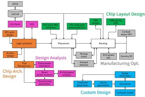
EDA challenges: Increasing chip complexity and costs
For decades, EDA has supported Moore’s Law by accelerating the development of advanced central processing units (CPUs), graphics processing units (GPUs), and various types of memory. Despite the impressive capabilities of EDA tools, a recent NVIDIA study found that up to 60% of a chip designer’s time is spent debugging or performing checklist tasks, such as tool usage, design specification, testbench creation, and root cause analysis. Additionally, technical documentation, processes, and design methodologies are often outdated or not fully shared across teams, further extending the design cycle.
The effects of these inefficiencies are worsened by the increasing complexity and costs of chip design at advanced nodes (5nm to 3nm). According to McKinsey & Company, designing a 5nm chip costs an average of $540 million and requires 864 engineer days — two to three times more than previous nodes. The rise of vertically stacked 3D multi-die systems (chiplets), devices with billions of transistors, and angstrom-scale structures further drives up design costs. Consequently, developing advanced-node chips for AI accelerators, high-performance computing (HPC), and autonomous vehicles could soon exceed $1 billion per design.
Accelerating time-to-market with GenAI and DRL
EDA companies integrate DRL and GenAI to address these challenges throughout their solution stacks. AI-based DRL trains agents to implement sequential decisions autonomously through trial and error in complex EDA environments. In contrast, by learning from extensive EDA datasets, GenAI creates new content such as text, images, or designs.
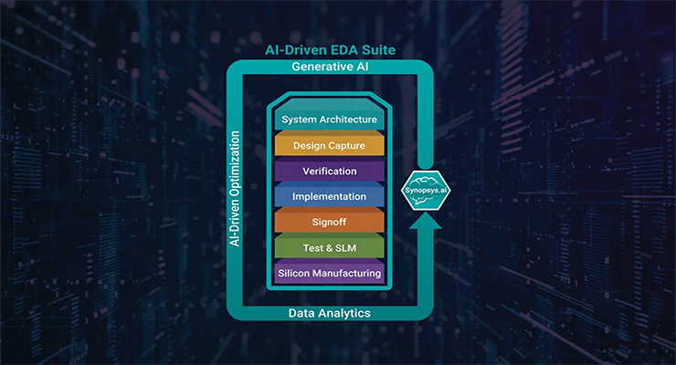
Many AI-based EDA tools leverage DRL to help chip design teams evaluate floorplans, review existing design libraries, and explore millions of potential design alternatives to optimise power, performance, and area (PPA). These DRL-based tools significantly shorten back-end processes from months to weeks, enabling small teams of engineers to complete complex design tasks efficiently. DRL improves yields and boosts overall production efficiency by identifying optimal configurations and reducing design errors.
Alongside DRL, GenAI EDA tools accelerate TTM by optimising system design processes and improving engineering and manufacturing methodologies. With advanced natural language capabilities, these GenAI-based tools integrate inference-based conversational intelligence into workflows. Engineers can automate the design of chips, electronic subsystems, and other semiconductor components using generative methodologies and specific prompts. Additionally, generating register transfer level (RTL) code from natural language specifications helps cross-functional teams efficiently navigate increasing chip design complexity.
Integrating GenAI throughout the EDA stack streamlines the creation and application of actionable insights from large datasets. It also automates the creation of shared product datasheets, technical manuals, and customised documentation. The continual expansion of internal datasets and optimisation of inference capabilities allow GenAI tools to provide crucial contextual recommendations during all EDA chip design process stages.
Optimising AI-based EDA with LLMs
LLMs significantly expand GenAI’s core capabilities for EDA by improving accuracy in natural language processing (NLP) and generation. Recent commercial and open-source LLM advancements streamline natural and programming language tasks across front-end, back-end, and production test phases. For example, LLMs automate EDA tasks such as code generation, responding to engineering queries, and assisting with documentation, including report generation and bug triage.
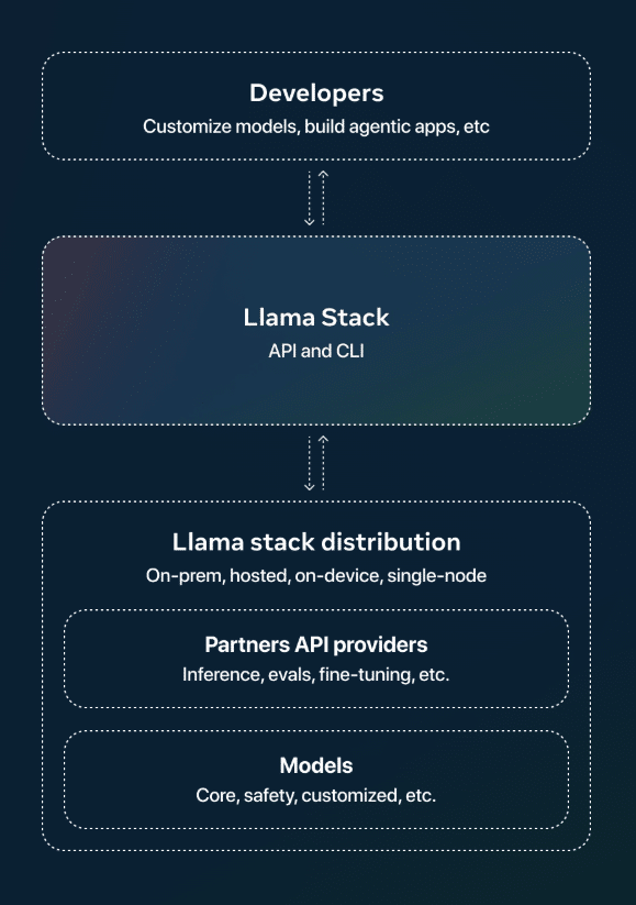
Another common use case for LLMs in chip design workflows is writing automation scripts to integrate EDA tools, reference methodologies, and proprietary logic. Foundation models like Code Llama efficiently generate and explain code in natural language. These models excel at Python code generation and can be fine-tuned for other scripting languages like Perl and Tcl, which are often used by EDA tools to interact with designs in a graphical user interface (GUI) environment. LLMs empower AI-driven engineering assistants to generate these scripts and facilitate natural language interactions with EDA tools, bridging the gap between engineers and design interfaces.
Customising EDA LLMs with RAG and fine-tuning
LLM accuracy depends on the quality and breadth of the data used for training. Due to the limited availability of semiconductor-specific data, LLMs can’t be effectively deployed out of the box in a production environment. Two customisation approaches are common for EDA and semiconductor applications: RAG and fine-tuning.
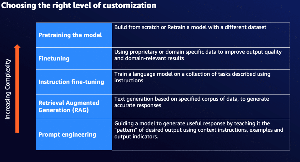
RAG relies on external data sources, such as document repositories or databases, to enrich prompts by converting documents and queries into numerical embeddings. This process enables relevancy searches within a knowledge library before appending relevant context to the foundation model (FM). In contrast, fine-tuning involves supplemental training of a pre-trained model on domain-specific data, modifying the model weights to improve its performance for specific tasks. Techniques like parameter-efficient fine-tuning and low-rank adaptation (LoRA) limit the extent of these modifications while adapting the model for specific EDA tasks.
A fully managed service such as Amazon Bedrock helps EDA engineers simplify the development of generative AI applications by providing access to a range of high-performing foundation models (FMs) from AI21 Labs, Anthropic, Cohere, Meta, Mistral, and Stability AI. Bedrock allows EDA engineers to experiment with multiple FMs using a single API for inference and switch models with minimal code changes. It also enables easy model customisation through a visual interface, supports RAG with integrated knowledge bases for seamless querying, and provides a powerful toolset for building applications like EDA engineering assistants.
Automated floor planning
Design engineers must optimise chip component layouts to meet multiple design constraints, such as performance, power consumption, and manufacturing costs. ML can help by analysing previously validated floor plans for similar chips and using that data to create optimised layouts. Reinforcement learning (RL), a type of ML, can learn from past designs and iteratively improve floorplan layouts by considering design factors like signal integrity, power distribution, and thermal management. This approach automates and refines the layout process, helping to improve productivity and reduce time-to-market.
An example of this is Synopsys’s application of ML in its IC Compiler II tool, where ML-driven macro placement technology predicts design metrics like congestion, wirelength, and timing. The tool learns from past results, exploring hundreds of floorplan options and selecting the most optimal layout.
Error log analysis for physical verification
The logs generated during chip verification are voluminous, often running into several gigabytes, and require human effort to review them and identify errors and warnings. ML algorithms can analyse the error text in reports and highlight key points to the user and also initiate actions by triggering a workflow to the relevant stakeholders. This can help improve design productivity and reduce design cycle time.
Several tools already use ML to improve physical verification. For example, Siemens’ Calibre nmDRC speeds up early-stage checks by running localised analysis — targeting only parts of the chip layout that have changed or are prone to errors. This approach enables faster feedback, better prioritisation of errors to fix and shorter debug cycles.
Copilot for design engineers
Chip design projects are complex and globally distributed, often involving multiple teams and specialists. Engineers frequently face delays when they depend on subject matter experts for resolving design and architectural queries. A generative AI-based design copilot can change that by offering real-time support, documentation assistance, and natural language interfaces to EDA tools. By integrating directly into engineers’ workflows, such copilots can accelerate development cycles and improve design quality.
The Synopsys.ai Copilot is an example of this: It integrates across the Synopsys EDA stack to enhance productivity, learn from ongoing projects, and adapt to organisational best practices.
Generative AI-based IP search assistant
AI can help in the selection of relevant IP and its reuse, one of the time-consuming but key activities involved in the design of semiconductors. Design engineers search for the most relevant IP from large repositories to integrate it into new projects.
While much research has been done on efficient IP management and several platforms exist, AI integration into these systems has been slow due to concerns over data sensitivity, fragmented and inconsistent IP data, complex licensing constraints, and the technical challenges of integrating AI into existing design workflows.
An AI-based IP search system can:
- Scan product requirements documents containing detailed specifications — such as operating conditions, power, performance, and hardware/software configurations — to extract relevant search parameters.
- Use semantic search capabilities to return matching IP records based on context and meaning, rather than exact keyword matches, enabling more accurate and relevant results even when terminology varies.
- Identify potential risks related to IP infringement and licensing, helping designers avoid violations of export control regulations or agreements with third-party IP vendors.
- Provide integration time estimates based on historical data, giving project teams a clearer picture of how long IP integration could take.
- Offer insights into expected design quality by analysing historical outcomes associated with similar IP usage.
- Assess potential cost implications for using specific IP blocks within a given project.
Considerations for AI adoption in chip design
AI is no longer a futuristic concept but a strategic part of semiconductor design. It can automate key processes like floor planning, verification, IP discovery and support real-time collaboration, improving efficiency across the design lifecycle. To achieve this, companies need to identify where AI can add the most value, such as in error log analysis and design verification. They should also assess data availability to support proof-of-concept projects and integrate AI smoothly with EDA tools to avoid disrupting workflows.
It is important to implement human-in-the-loop systems that provide engineers with insights while maintaining oversight and accountability. Continuous learning and iteration will help AI systems improve over time, offering more tailored solutions and speeding up design processes. This approach helps semiconductor companies make better use of AI within their existing operations.
We are at a pivotal point in EDA, as the semiconductors and PCB systems that underpin critical technologies, such as AI, 5G, autonomous systems, and edge computing, grow increasingly complex. The traditional EDA workflow, which includes architecture design, RTL coding, simulation, layout, verification, and sign-off, is fragmented, causing error-prone handoffs, delayed communication loops, and other roadblocks. These inefficiencies prolong cycles, drive up costs, and intensify pressure on limited engineering talent. The industry urgently needs intelligent, automated, parallelised EDA workflows to overcome these challenges to keep up with increasingly aggressive market demands.
AI as the critical enabler of next-gen EDA
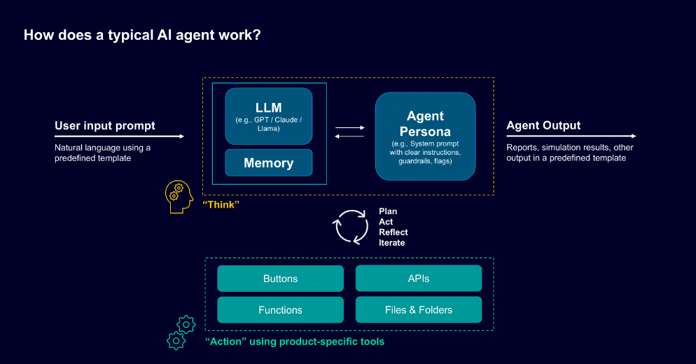
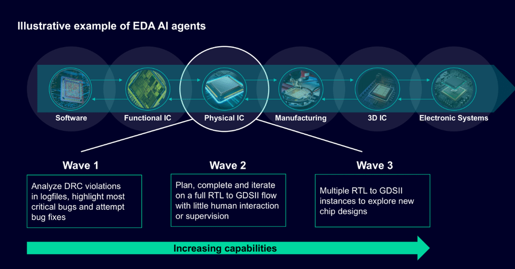
AI is becoming essential across industries, and EDA is no exception. Historically, Machine Learning (ML) and Reinforcement Learning (RL) have enhanced tasks like layout optimisation, simulation acceleration, macro placement, and others, in addition to leveraging GPUs for performance boosts. Generative AI has recently emerged, enhancing code generation, test bench synthesis, and documentation, yet still requiring significant human oversight. True transformation in EDA demands more autonomous AI solutions capable of reasoning, acting, and iterating independently. Fully autonomous AI agents in EDA will evolve progressively in waves, each building upon prior innovations and demanding multi-domain expertise. We have identified three distinct waves of EDA AI agents, each unlocking greater autonomy and transformative capabilities.

Wave 1: Task-specific AI agents
The first wave of AI-powered transformation in EDA introduces task-specific AI agents designed to manage repetitive or technically demanding tasks within the workflow. Imagine an AI agent acting as a log file analyst, capable of scanning vast amounts of verification data, summarising results, and suggesting corrective actions. Or consider a routing assistant that works alongside designers to optimise floor plans and layout constraints iteratively. These agents are tightly integrated with existing EDA tools and often leverage large language models (LLMs) to interpret instructions, standard operating procedures, and other natural-language comments. Due to their specialised nature, each phase in the EDA workflow might require multiple such agents. Consequently, orchestration becomes key: a human engineer oversees this fleet of AI agents and must intervene frequently to guide these specialised agents.
Wave 2: Increasingly autonomous agentic AI
Wave two introduces agentic AI, which are solutions that are no longer just reactive but proactive, capable of sophisticated reasoning, planning, and self-improvement. These differ from AI agents, which specialise in a specific task. Agentic AI solutions can handle entire EDA phases independently. For example, an agentic AI assigned to physical verification can conduct DRC and LVS checks, identify violations, and autonomously correct them by modifying the design layers—all with minimal human input. These Agentic AI solutions also communicate with one another, passing along design changes, iterating in real time, and aligning the downstream steps accordingly, making these solutions even more powerful as they enable an iterative improvement cycle.
Furthermore, Agentic AI solutions can deploy multiple task-specific AI agents described in Wave 1, thereby not requiring fine-tuning for every specific task and instead requiring fine-tuning of reasoning, planning, reflection, and orchestration capabilities. An EDA engineer or a purpose-built supervisory agentic AI typically oversees this orchestration, adapting the workflow, resolving conflicts, and optimising outputs. Essentially, imagine a 24/7 design assistant that never sleeps, constantly refining designs for performance, power, and area. This is not a future vision—it is a near-term possibility.
Wave 3: Collective power of multiple AI agents
The third wave isn’t just about making individual AI agents or an agentic AI solution necessarily smarter—it’s about scaling this intelligence. A powerful multiplying effect is unlocked when we move from a 1:1 relationship between engineer and AI solution to a 1:10 or even 1:100 ratio. Imagine, instead of relying on a single instance of an AI agent or even an agentic AI to solve a problem, you could deploy dozens or hundreds of agents, each exploring different architectures, optimisations, or verification strategies in parallel? Each instance follows its plan, guided by different trade-offs (e.g., power vs. area in PPA optimisation). At this stage, the human role evolves from direct executor to strategic supervisor, reviewing outcomes, selecting the optimal solution, or suggesting fundamentally different design approaches. The result is exponential acceleration in both new product innovation and faster design cycles in each of the new as well as products. Problems that took weeks to debug can now be explored from multiple angles in hours. Design ideas previously dismissed due to resource constraints can now be pursued in parallel, uncovering groundbreaking opportunities that would have otherwise remained largely undiscovered.
Both individuals and organisations will reap the transformative benefits of AI
As we enter this new EDA era, agentic solutions are going to shape how individuals and organisations work. At the individual level, chip designers gain productivity as AI takes over repetitive tasks, freeing them to focus on creative problem-solving. Micro-teams of AI agents will enable rapid exploration of multiple design scenarios, uncover superior designs and speed up tape-outs, thereby augmenting human expertise with faster AI-led execution. At an organisational level, AI-driven EDA solutions reduce time-to-market, accelerate innovation, and foster rapid development of cutting-edge products. More importantly, AI democratises expertise across teams and the entire organisation, ensuring consistent, high-quality designs regardless of individual experience, enhancing competitiveness. In conclusion, EDA AI will transform workflows in the next few years, greatly boosting productivity and innovation.
Many EDA companies integrate GenAI and DRL capabilities throughout their solution stacks to help semiconductor companies efficiently design chips at advanced nodes. LLMs significantly expand GenAI’s core capabilities for EDA by improving NLP accuracy. For example, LLMs automate EDA tasks such as code generation, responding to engineering queries, and assisting with documentation, including report generation and bug triage. Together, these AI-driven technologies accelerate TTM, improve yields, and lower costs over time.
Challenges and future directions
AI models heavily depend on large, high-quality datasets to perform effectively in chip design. However, obtaining labelled data specific to semiconductor design is difficult, and bias in training data can lead to suboptimal designs, especially in cases with unique requirements. To proactively mitigate this, it is essential to diversify training datasets, ensuring AI models generalise well across a broader range of scenarios and improve chip design quality.
One of the primary concerns with AI in chip design is the black-box nature of some models. While AI can optimise performance and power, engineers play a crucial role in verifying the rationale behind AI-generated designs. This active involvement is essential to address trust issues arising from the lack of transparency, and it also ensures that the adoption of AI in critical design workflows is not hindered.
Although AI has excelled in tasks like placement and routing, scaling these models to handle diverse chip architectures, including analogue and mixed-signal designs, remains challenging. Additionally, the limited talent pool with expertise in semiconductor design and AI further slows adoption. Addressing this skill gap is vital for the seamless integration of AI into chip design processes.
The future of AI in chip design lies in explainable AI (XAI), cross-domain collaboration, and adaptive models. XAI will help engineers understand AI decision-making processes, boosting trust and efficiency. Moreover, AI will increasingly augment EDA tools, enabling real-time optimisation across the entire design lifecycle. Adaptive AI models will iteratively refine designs based on real-world performance, positioning AI as a true co-designer.
How AI will transform the semiconductor industry by 2030: Key trends and predictions
Artificial Intelligence (AI) is not just transforming the world of software – it is rapidly reshaping the semiconductor industry from the inside out. Over the next five years, AI is expected to have a massive impact across chip design, manufacturing, supply chain management, and market competition. In this post, we’ll explore how AI is driving this revolution, what changes we can expect, and what this means for companies and professionals in the semiconductor space.
AI-powered semiconductor design: Faster, smarter, and more efficient
One of the most immediate and visible impacts of AI is on chip design workflows. Traditionally, semiconductor design has been an extremely time-consuming process involving complex manual steps from RTL design to GDSII. AI is now automating and optimising many of these steps.
- Faster design cycles: AI-powered electronic design automation (EDA) tools like Synopsys DSO.ai and Cadence Cerebrus are cutting design timelines by automating physical layout optimisation, verification, and design space exploration.
- Smarter architectures: AI models can explore millions of design permutations to improve power, performance, and area (PPA) trade-offs, enabling the creation of more efficient and advanced chips.
- Generative AI in design: Generative AI is entering the semiconductor space, helping engineers explore new microarchitectures and generate design blocks faster than ever before. It is also playing a crucial role in generating test benches covering different scenarios, including corner cases, to achieve higher verification coverage.
In the coming years, companies that integrate AI-based design tools will release chips to market faster, with better performance, gaining a significant competitive edge.
Surge in AI-specific chip demand
One of the most significant trends shaping the next five years is the explosive growth in demand for AI-specific chips. This includes GPUs, NPUs, AI accelerators, and domain-specific processors for edge computing.
- Boom in AI chip sales: AI chips for training large models and running inference at the edge will dominate semiconductor growth.
- Rise of specialised hardware: Custom AI accelerators and neuromorphic chips will become more common, offering lower latency and energy-efficient AI processing.
- Increased competition: Cloud providers, automotive companies, and consumer electronics brands will all develop or adopt specialised AI hardware to keep up with market demands.
AI will not only shape how chips are designed but also what types of chips dominate the market.
New business models and industry dynamics
As AI reshapes the semiconductor ecosystem, business models and partnerships are also evolving.
- EDA-as-a-service: Cloud-based, AI-augmented design platforms will make cutting-edge chip design accessible to smaller players.
- Foundry partnerships: Major foundries like TSMC, Samsung, and Intel Foundry Services will focus on offering AI-optimised process nodes and advanced packaging for chiplet-based designs.
- Shift toward AI-centric IP: There will be increasing demand for IP blocks optimised for AI, including network-on-chip (NoC) architectures, low-latency memory, and energy-efficient interconnects.
The semiconductor landscape will see more collaboration, cloud integration, and a focus on AI-first architectures.
Risks and challenges ahead
Despite its advantages, the growing role of AI in semiconductors comes with new risks and challenges.
- Skill gaps: Heavy dependence on AI-driven tools may lead to a shortage of engineers skilled in manual chip design and debugging.
- Security concerns: Cloud-based EDA and AI model sharing increase the risk of intellectual property theft and data leaks.
- Verification complexity: AI-generated designs may be less intuitive for human engineers to verify, potentially increasing functional risk.
The evolving talent landscape
The semiconductor industry will demand new skill sets:
- Engineers will need to understand both semiconductor fundamentals and AI/ML workflows.
- Cross-disciplinary expertise will be in high demand, especially for those who can bridge AI, VLSI, and systems engineering.
The impact of AI on the semiconductor industry is no longer speculative; it is already here and growing. Companies that embrace AI-driven design, smart manufacturing, and AI-centric business models will lead the charge toward faster innovation and greater market share. Those who fail to adapt risk being left behind in an industry that is moving faster than ever before.
The next five years will not just be about making chips better – it will be about redefining how chips are made, delivered, and integrated into the AI-powered future.
By: Pournima P R has been working as a Lecturer for 5 years in the ECE Department at B E S Institute of Technology, Bengaluru.