 With the increase in usage of smartphones, opportunities for applications using mobile phones have also increased. This coupled with connectivity options such as Bluetooth and Near Field Communication and add-on devices to the phones have become very popular as these offer unique solutions. These devices can work as a simple radio-frequency identification reader to a sophisticated medical device. While the devices use conventional electronic circuitry, product packaging and usage are completely different. Right from the material used to the product shape and size have to be carefully selected to ensure safety of the wearer.
Most of these devices are small and irregular in shape. Engineering these needs special skills and manufacturing these needs special equipment and processes. Designers need to follow special design practices for wearable designs to be realised as successful products. There are very few books available for designers to design wearable products. This article tries to help design engineers to get an overall view of the design and manufacturing process of wearable devices.
Since wearable devices are normally made in large numbers and are miniature in size, use of contract manufacturing is recommended. The focus is on the design process and what designers should look for when they design wearable devices to be made by contract manufacturers. While this list is not exhaustive, it gives a fairly good view of the complexities involved in the wearable device design.
Defining wearables
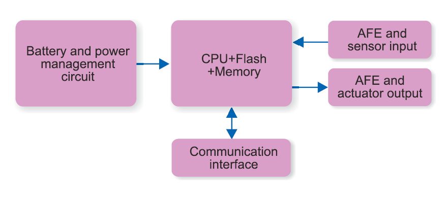
Wearable devices are no different from classic embedded systems that we are all familiar with. Block diagram of a wearable device is shown in Fig. 1. It has following four blocks:
1. Power supply and management circuit
2. Core processor
3. Analogue interface [analogue front-end (AFE) covering sensor inputs and actuator outputs]
4. Communication interface (wireless and wireline)
What differentiates wearable devices from conventional embedded systems is the power management circuitry. Most wearable devices are battery-operated (either primary or chargeable) and need special circuitry to control power consumption.
Power management circuitry alone cannot optimise power consumption. It is the combination of the power management circuit and the device software in the system that results in optimal power consumption.
To a large extent we can say that, the processing power needed by wearable devices is very low, as most devices just collect data from sensors, store and send it to the central application for processing. The central application could be a smartphone or, in the case of the Internet of Things, cloud-mounted software. This is essentially done to ensure that the battery lasts long and data is processed in a central location by a more powerful processor.
Most integrated circuits (ICs) use very high-speed complementary metal-oxide semiconductor (CMOS) technology. In CMOS technology, power consumption of an IC goes up as the operating frequency of the processor goes up. So most wearable devices use low-speed controllers, and sections of the microcontrollers (MCUs) can be shut down or operated at a low speed when not in use.
We also need to remember that, some wearable devices that are used in medical applications (like insulin pumps or carry-on ECG probes) need to be designed in a controlled way, as these are approved by regulatory bodies like FDA/CE. Most device vendors do not recommend their devices for medical usage to avoid getting sued in case of any failure.
Classifying wearables
Wearable devices can be classified into the following four major categories:
Sports and fitness. Sports and fitness devices primarily track movement (using accelerometers) and, in some cases, heartbeat. While worn, these normally track motion and not body parameters.
Personal health monitoring. These devices track heartbeat, body heat, blood oxygen (SpO2) and ECG (single or 3-lead) signals and, in some cases, have special sensors. These devices normally track body parameters and therefore need to be highly reliable, as readings may be used for lifestyle adjustments.
Tracking and monitoring. These devices have GSM/GPS functions and are primarily used for tracking the wearer, mostly in geo-fencing applications.
Medical applications. These are high-end devices that are typically worn by patients who need controlled dosages, periodically. These devices are regulated and controlled by regulatory agencies. For this, manufacturers need to follow strict processes during development and manufacture. Importance of the rigid process is to ensure that these devices are traceable and, in case of problem, the root cause can be analysed up to the component level.
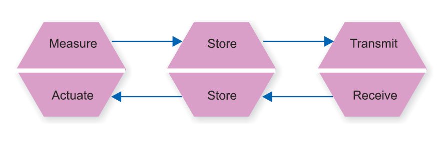
Most wearables can handle very low analogue signals and therefore have substantial analogue circuitry to process these. These are also real-time devices and synchronise their operations to the time or date for data collection/measurement. Their functionality can be represented by the flowchart shown in Fig. 2.


Essential design elements
Let us now take a look at some generic design elements that impact a product. These impact both design and manufacture of wearable devices. A product’s performance, its manufacturing and usage characteristics all depend on how well the design is done.
First, let us understand the life cycle of a wearable product so that it is easy to understand the issues involved and how these can be addressed. Fig. 3 shows the typical life cycle of a wearable device. A device essentially goes through four major phases as shown in the figure. While the design, manufacture and use phases are sequential, support phase is basically concurrent, addressing the manufacture and use phases. The reason for taking a life-cycle based approach is to show how designs need to address issues that crop up in subsequent stages.

Design phase. During this phase there are a few things that designers need to know for a successful wearable design. These are:
1. Almost all wearable devices have sensors that use a very low signal level. This necessitates that the designers be very strong in analogue and mixed signal (combination of analogue and digital signals) circuit designs.
2. Since most wearables are battery-operated, designers need to be conversant in low-voltage analogue designs as well as power-conversion techniques (like boost regulators).
3. Intricate knowledge of MCUs used and how their power management is implemented is essential. To reiterate, an increase in processor speed increases power consumption, so managing the processor speed dynamically is crucial for optimal consumption of power.
4. In-depth understanding of the battery types used, their charging characteristics, their behaviour against temperature variation, safety limits and different charging circuits is a must. It is important for designers to know circuit simulation tools like Simulation Program with Integrated Circuit Emphasis (SPICE), as with these tools, they can evaluate the circuitry before committing to the design.
One important thing that a designer needs to keep in mind is the accuracy of the models used in simulation. A wrong or an inadequate model will produce wrong results.
5. With most wearable devices being small in size, the impact of components on neighbouring components in the PCB is very critical. A good example would be the vibrators used in a wearable device that produce strong physical vibrations and also have a magnetic field. Any device nearby that is sensitive to stray magnetic fields can produce wrong results when the vibrator is working.
Designers tend to miss issues like these and struggle to solve them when the actual product runs into trouble. So it is important they understand the components used along with their characteristics.
6. With miniature designs come miniature components and their own specific challenges. Components like capacitors and coils have precise dimensions and need to be placed correctly.
Another key component that most designers underestimate is miniature connector. While there is no dearth of miniature connectors, these come with a big restriction on the number of insertions. This is due to connector geometry. In most cases, the number of insertions is in the range of 30 to 40 cycles.
If the assembly process takes more insertion cycles, it can reduce the active life of the connector. (When I was designing a movie camera, we had three to four connectors that were getting cycled 20 to 30 times during the assembly process. The connectors started failing when the final system assembly was done, leading to a complete revamp of the assembly and test process.)
7. Designers should completely understand use cases. If their devices need special chargers or special supplies, they need to plan that as part of the product. With proliferation of USB based charging, most devices tend to supply the product without chargers. However, all chargers are not the same. So if your device is expecting a special treatment, then that has to be provided. If not, the device should be tested for chargers available in the market to ensure there are no surprises.
8. Most wearable devices are waterproof (in technical jargon these are called IP67 compliant). This essentially means that the device enclosure design has to be leak-proof up to a depth of at least 50 metres when submerged in water. This needs skill and experience. The manufacturing process should be able to reproduce protection for each piece that is manufactured. It is advisable that a relevant subject matter expert is hired as a consultant to review the design and ensure the packaging is leak-proof.
9. Another challenge that designers face is: How will the software team develop the software if the wearable device design is going to take time to get the prototypes ready?
I suggest that, make the wearable circuit in a large PCB format with bigger components that are used in the design and have test points, so that software developers get the actual target hardware to develop software and do not have to wait for the final miniature version. I have found this approach very useful as it reduces development time considerably despite an additional investment in the hardware.
10. With size being the premier constraint, sometimes volume and shape of the product forces designers to use a complex architecture for the design. Most wearable devices today use a mix of PCBs and flexible circuits to realise the final design. This approach needs a good understanding of these two materials and also how to use these.
The contract manufacturer (electronic manufacturing service or EMS) must be identified as soon as the design is started. Challenge with flexible PCBs is that, every time you revise these, there is substantial upfront expense (non-recurring expense) involved, and multiple revisions can drive up development costs.
Manufacturing phase. The second important stage is the manufacturing phase. A product will be successful only when the design and manufacturing teams work together. When wearable devices are designed, it is important that, at the start of the project, the EMS partner is decided. Let us see some challenges that wearable products face in this phase.
A conventional SMT process invariably is inadequate for wearable devices due to the following reasons:
1. Miniature size of the product with very less volume and space available inside the enclosure leads to a complex assembly process.
2. In most cases the battery consumes the major volume, leaving little space for the electronics. This leads to very tight packaging and, unless adequate precautions are taken, yields can be a challenge.
3. The smaller PCBs and the use of flex cables sometimes calls for development of special jigs and processes like ultrasonic soldering of flex cables.
4. With reduction in size, many times a product has to be manufactured using packing techniques like chip on board (CoB); normal IC packages and dies that are packaged in standard packages with leads increase the volume manyfold as compared to using the die directly. In a CoB process, the die is directly soldered to the PCB and requires special equipment. Unfortunately, this technique is the only way by which product volume can be reduced substantially.
With component size being the biggest deciding factor, it is important that the designer works with the supply chain of EMS vendors to select the right package size so that, apart from the realisable design, availability of components is also guaranteed. EMS vendors usually have a very good supply chain. They ensure there are no shortages, so that increased lead time does not impact the production schedule.
In the second part of this article, we will discuss the testing phase, wearable system software and development phase.
S.A. Srinivasa Moorthy is CEO, Andhra Pradesh Electronics and IT Agency


