


In the first part of this article we defined and classified wearables, and covered the designing and manufacturing phases of the life cycle of a wearable product.
In this concluding part we look at the testing and support phases, wearable system software and development phase.

Testing phase. The third important aspect is how the assembled board and product is tested. Conventionally, PCBs have test points (these are PCB pads of specific dimensions). Testers known as beds of nail testers test these assembled PCBs. These testers have a set of spring-loaded nails that are positioned against each test point. The test electronics under the control of test program tests every node by applying a stimulus and checks the response of the node and compares it with the response of a good PCB (known as gold board).
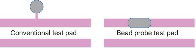
This type of testing is good when PCB sizes are not too small. However, most wearable devices use miniature PCBs and flex cables, and testing of these boards calls for special techniques. Such boards do not have space for test pads as these are crammed with components. So a frequently-used technique known as bead probe testing is used. Fig. 4 shows the conventional test pad and bead probe test pad for better understanding.
In this test method, instead of a separate test pad (typically a pad of 40mil diameter), a bead is formed (a solder bead of 20mil diameter) on the PCB trace and the tester probe probes this point and tests the PCB. This enables miniature PCBs to be tested without much difficulty. However, to implement this testing, designers have to prepare the PCB with this feature. And they need to work with the test engineering team of the EMS partner to locate the probes for proper balancing of the PCB when testing is carried out.

Another method used, when the wearable device has only one CPU (which is normally the case), is called JTAG testing (this needs about five to seven test points, regular or bead probes). It is used to test the entire assembled PCB. This technique is popular and costs low but needs the designer’s time and efforts.
One challenge in JTAG method is, if the controller IC is brand new and is being used in the product for the first time, most chip vendors may not have the required JTAG test file (known as Boundary Scan Description Language or BSDL file) ready. This can happen when the company that makes the wearable device expects a large volume and goes for a dedicated custom application specific integrated circuit, making JTAG testing difficult initially.
Finally, since most wearable devices measure very low analogue signals, these need to be calibrated once the product is assembled completely. This is the responsibility of the design team, and they need to train the EMS partner on the calibration process as well as the calibration equipment. Many a time this is missed and product shipment is delayed due to difficulty in calibration.
Use phase. This phase is where the product actually goes into the hands of the users.
One big challenge that designers face is how exhaustively they have covered the product use cases (right way of using the product) and misuse cases (wrong way of using the product). While most designers are able to cover the right use cases well, they fail to do so for the wrong use cases. In fact, testing for wrong use cases is a unique feature that medical device developers must use when developing medical devices.
Most designers think that by displaying disclaimers about wrong usage they can cover their liability. But the risk is that, there are corner cases where products fail despite being used correctly.
Let us take the case of a wearable that has a magnetic-field-sensitive sensor. In the normal usage, it does not get impacted, but if a user wearing the device goes near an equipment that has a high magnetic field (like a big transformer), the wearable can fail due to the sensor being impacted by the external field. A disclaimer cannot adequately describe this situation, and the user may not be able to avoid going near the system. In these cases, product shielding needs to be designed so that no external magnetic field can impact the wearable device.
Second issue is the biocompatibility of the material used. Since the wearable device will be in contact with users’ skin for extended periods, materials used should be safe and not cause any skin problems. This poses challenges in terms of costs and processes. Biocompatible materials are sometimes expensive and also need special processes to manufacture. Designers need to factor this in the design phase itself. This problem is acute when the product enclosure is metallic.
In addition, if devices have probes that are metallic and need to touch the skin, these invariably need special gels to ensure good contact, and the materials also need to be safe for use.
One of the frequently faced problems is water ingress inside the wearable devices. In many cases, initially, the product remains waterproof but sometimes seals that were used for prevention of water ingress wear out over a period of time, in turn, losing the ability to prevent the water from entering. Designers need to factor this as well and ensure that proper material is selected.
Designers can define the product usage period (useful life) so it can be discarded once the prescribed time is over. This works well when the product cost is low, but if the product is expensive, a proper mechanism of inspection and preventive check is a must if the design has aging issues. This is especially true in the case of a wearable device used for medical applications, where the product cost is high and customers tend to use it for a longer period.
Finally, sometimes wearable devices may have consumables such as gels, pads and wipes. These have to be consistent and their tolerances have to be within the specified limits. Many a time, as time passes, cost pressure takes precedence and companies switch over to a low-cost material, which impacts the product, leading to failures. This happens also when some critical inputs are forgotten or missed out. This must be kept in mind.
Support phase. Most wearable devices are use-and-throw types at the end of their life or when gone faulty. This is due to the low cost of the products and high repair costs. Product manufacturing process in this case uses a specialised procedure that cannot be replicated in the repair centre.
However, when the product is expensive (like some medical equipment), it must be supported and would need to be repaired. If this is a requirement from the beginning, designers have to plan and implement this in the design phase itself. They need to clearly define a process, which will achieve the same type of assembly that is done at the manufacturing line, ensuring product integrity and reliability.
An important support issue is software upgrade; most wearable devices when launched do not have the full complement of the features and may also have bugs. Designers need to make provisions for the following two important aspects:
1. Provide a reliable communication mechanism through which the software can be upgraded.
2. Provide adequate internal memory so that if the upgrade process fails, the product can still work with an earlier version of the software.
Both of these provisions should be planned in the design phase and implemented.
Another way to tackle this issue is to keep the software functionality to bare minimum and carry out all complex operations either on the central application or on a smartphone, depending on where the application is running. This also ensures that cost of hardware is kept low and the software is simple, so that it can be tested and does not need an upgrade, if properly tested. With the option of software upgrade being done in the application, large-volume device software upgrade related issues can be reduced.
Wearable system software
Software for wearable devices is completely dependent on design consideration, functionality of the device and controllers used. However, there are certain generic elements that software developers need to keep in mind when deciding the software architecture of wearable devices. Following guidelines should be helpful when deciding on software architecture:
1. Use a standard-platform based architecture so that maintaining the software is easy.
2. Even when a simple two to three tasks functionality is needed, use of a real-time scheduler (kernel) allows predictable performance and ensures consistency in data, when data needs to be collected for a longer duration and data volume is high, along with time stamp. This particular aspect is very successful in a wearable device design, especially when healthcare functionality is implemented.
3. For complex functionalities, a Linux based platform is advantageous. Customising the Linux kernel by removing unwanted drivers creates a compact footprint as well as tighter and verifiable codes.
4. Implement the power management function specifically for your hardware by measuring the power consumed and understand the battery that is being used. Many a time, using a generic power management function results in sub-optimal performance. Knowledge of processor core and the memory used is important for implementing the power management function. A wearable device’s success mostly depends on its battery life.
5. Ensure that the software is upgradable and also has sufficient headroom for code expansion in the hardware. It is advisable to have only about 70 per cent memory to be occupied when releasing the product. When the memory usage reaches 90 per cent, you can revise product hardware with a higher capacity.
6. Since most wearable devices store data before these are shipped out, ensuring a reliable mechanism that occupies optimal space to store data is important. For example, if the position of 1-switch data uses a byte, packing 8-switch data in one byte can save huge memory area.
7. C based application is suitable for real-time and critical time-sensitive applications. With proliferation of Java, designers tend to use it but for power-sensitive and performance-critical applications, languages like C are better suited.
Development process
While lack of a process may be fine when the product volumes are small, as volumes increase it is risky not to have a process in place, especially in the case of wearable devices. Since most wearable devices interact with humans, and humans use these in their daily regimen, having design decisions documented by following a process will help avoid any future litigation. Let us see an example.
You have designed a wearable device where you have calculated the battery life of 2.5 years and you certify that the device will work for two years before requiring a replacement. If a user continues to use this, let us say for three years, and the device fails and the user sues the company, you should be able to show your documentation to prove that your device is meant to work for two years and at best 2.5 years, and anything beyond is not guaranteed.
Most medical devices have a well-documented process defined by ISO 13485 standard, and design process documents are stored till the product is withdrawn from the market. These files are known as design history files. The medical device development process is exhaustive and takes time and effort to create and maintain. While wearable devices need not have such a detailed process, there are a few documents that when created will help designers and the company to manage the product successfully.
Given below are the essential documents that designers need to create and maintain for a successful wearable device:
Product requirement document. This document captures every product feature that will be implemented. Every feature is uniquely numbered so that each requirement can be tested and validated.
Material selection document. This document captures the details of all materials considered for product packaging and their characteristics, and the material chosen and technical reasons for the same.
System architecture document. This document covers product architecture at the highest level (as block diagrams), the specific device chosen and the reason for that choice. This should also cover software architecture and software components chosen and the reason for choosing these.
System safety analysis document. This document analyses the safety features and the impact on the user and its safety. Let us say, due to some hardware problem the wearable device starts reading double heartbeat as normal. In this case, the software should have a feature that compares the reading with standard set limits and, if data is out of bound, raises an alarm. This comes in handy when the wearable measures body parameters and users use it for their daily health monitoring. So if wrong data is read by the system, it should not force users to change their daily routine due to this error.
Critical design decision document. This document captures all critical design decisions covering selection of parts to the way PCB has been laid out, test strategy and test hooks, among others. This document comes in handy when the next-generation product has to be designed or when product revision has to be done.
Test strategy document. This is a key document where the test strategy adopted for testing the PCB, product and calibration procedure and details of the tester are recorded. It helps in managing the yield as well as improving productivity. Above all, in case of failure, this document ensures isolation of the problem found in the manufacturing line.
Product master record. This document captures the product’s serial numbers and corresponding test results with the measurement so that when failure due to aging happens, the reasons can be tracked back to the batch and the process involved. It is typically created out of manufacturing line and, during contract negotiation, data capture has to be put in contract.
The primary idea behind this article was to demystify wearable devices and the essential characteristics these should have. While this article does not serve as a comprehensive guide, it does help to understand the intricacies of a wearable device design and how it can be designed for success.
Concluded.
To read the first part of the article: click here
S.A. Srinivasa Moorthy is CEO, Andhra Pradesh Electronics and IT Agency