


NOVEMBER 2012: It is said that with the exception of Dresden (hub for companies like GlobalFoundries and now Infineon with its recent acquisition of Qimonda’s assets), Europe might find itself open to attack on 450mm fabs, given its predominantly 200mm/150mm manufacturing base.
Europe’s chip companies will be subjected to a constantly ongoing closure and restructuring effort, damaging the employees’ morale and affecting the costs and productivity. Finding and keeping good operations personnel will be very difficult indeed, given this business strategy is an operations career’s dead-end.

Future Horizons has long stated that the ‘fab-smart’ strategy remains the only true solution. This means continuing to build in-house state-of-the-art fabs while outsourcing a modest amount (5-15 per cent maximum) to foundries in order to smooth the supply and demand peaks and build external fab demand high enough to justify equipping the next module of in-house expansion.
In this way, any expansion in capacity enters production ‘fully loaded’ from the beginning whilst simultaneously improving response time to near-term demand fluctuation. The foundries do not like this option of course, but this is the only real competitive reality for integrated device manufacturers.
There is a parallel opportunity for an European-based 450mm wafer fab focused on more mature technology node processing.
In 450mm process, there have hardly been advances in Europe as far as silicon readiness (scratches eliminated and particle count dramatically reduced) is concerned, according to Malcolm Penn, chairman and CEO, Future Horizons. “They have not made anything beyond a few sample wafers yet.”
As for the particle, edge and thin-film measurements capabilities required for 450mm fabs, he adds that this is just a part of the whole transition process. All has to be ready in time for the first module.
Where will the fabs be?
So when are the first 450mm fabs likely, and where? Intel has announced that its first 450mm pilot plant will be at Hillsboro in Oregon in the new D1X fab. It will be used to debug the production process before moving it to other high-volume sites.
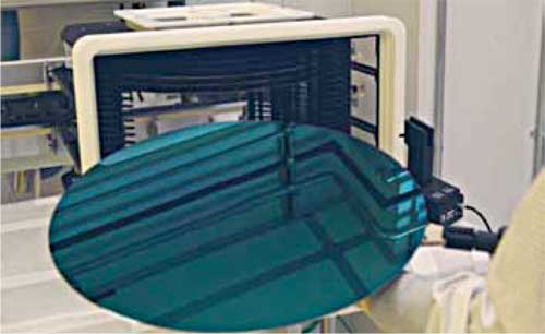
[stextbox id=”info” caption=”What is 450 mm?”]
The global semiconductor industry is going to make a major transition from producing 300mm wafers to 450mm wafers. This move to 450mm wafers also means that companies can set up 450mm fabs (fabrication units) that will lead to reductions in die cost, and later, production cost.
A wafer is a thin slice of a semiconductor material, such as a silicon crystal, used in the fabrication of integrated circuits (ICs) and other micro devices. It is believed that 450mm wafers will cost less per unit output than 300mm wafers. It is also said that 450mm production will make it easier to stay in the game because it is cheaper. The 450mm fab and wafer could become a reality by 2018.
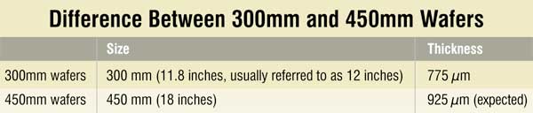
[/stextbox]
Currently, this fab is in a very early construction stage, planned for a 300mm line initially and a 450mm pilot line sometime later. The second plant will be in Arizona. The location of the third plant is yet to be decided. It could be in the US, Israel or Ireland.
Only the University of Albany’s College of Nanoscale Science and Engineering (CNSE), IMEC, Intel (Oregon), Samsung and TSMC are expected to be able to research and develop 450mm wafer processing during this decade.
Fab gameplan
Intel is the prime driver in the move to 450mm wafer processing. It has announced its intent to run in the first line on a proven process/IC design combination at the 15nm node before moving to 11nm once everything is proven capable of operating at this node properly.
It will be interesting to see how TSMC allocates wafers on its first 450mm fab and how much it charges for them. TSMC is perhaps the most complicated 450mm business case, given that its first 450mm product will have to be a logic IC. The key decision will therefore be whether the first 450mm process will be high-speed or low-power.
Samsung’s first 450mm fab is expected to be a memory fab. It’s not certain whether this would be for DRAM or Flash.
Industry observers believe that the first 450mm wafers will be produced at node n-1, but they will be flipped to node ‘n’ as soon as the 450mm platform bugs are ironed out with comparable or better wafer fab yields and performance than the established past-practice.
This might be sooner rather than later for Intel, given its high-performance fab business model, and later rather than sooner for TSMC, where stable yields and low cost are the key driving factors. A few fabless semiconductor firms, though, are expected to be prepared to share the potential die cost risk with TSMC in order to benefit from the early 450mm experience.