




A new 3D chip stacking method developed in Japan promises to revolutionize AI and high-performance computing with faster data transfer, reduced power consumption, and compact integration.
In a significant leap for semiconductor technology, researchers from Science Tokyo have introduced an advanced 3D chip integration approach aimed at delivering high memory bandwidth and ultra-low power consumption for next-generation computing systems. Their work was recently showcased at the 2025 IEEE Electronic Components and Technology Conference (ECTC).
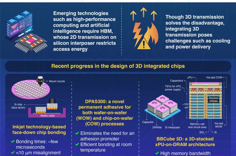
Traditionally, system-in-package (SiP) designs use 2D chip placement via solder bumps, which restricts further miniaturization and performance scalability. To address these challenges, the team developed a cutting-edge chip integration framework named BBCube, based on a 2.5D/3D stacking approach. This architecture features processing units (xPUs) stacked directly above DRAM modules, enabling shorter interconnects and faster data transfer.
To make this architecture viable, the researchers tackled three critical areas. First, they created a face-down chip-on-wafer (COW) bonding process using inkjet technology and selective adhesives. This enabled the precise and rapid mounting of over 30,000 differently sized chips on a 300 mm waffle wafer with chip-to-chip gaps as narrow as 10 micrometers—and bonding times of under 10 milliseconds per chip.
Second, to support the mechanical and thermal demands of ultra-thin stacked wafers, they formulated a novel adhesive named DPAS300, built on an organic–inorganic hybrid structure. This material offers strong thermal stability and can be used across both chip-on-wafer and wafer-on-wafer bonding processes.
Lastly, to ensure stable power delivery and high-speed communication within the stack, the team implemented a new power distribution highway. This includes embedded capacitors between layers, through-silicon vias, and redistribution layers to reduce energy loss and suppress power noise to below 50 mV.
By reducing data transmission energy to just 5–20% of conventional systems, this 3D integration technology opens doors for more efficient AI hardware, HPC systems, and edge devices. The innovations from Science Tokyo could mark a foundational shift in how chips are packaged and powered in the AI-driven computing era.


