


A new programmable photonic chip eliminates static power consumption while enabling electrical control, promising energy-efficient AI computing, faster prototyping, and scalable optical systems for next-generation electronics and data infrastructure.
A newly developed optical microchip developed by Wayne Gillam, University of Washington – Department of Electrical & Computer Engineering, that consumes zero static power while remaining electrically programmable, could significantly reshape energy-efficient computing and photonics-based electronics. The breakthrough addresses one of the biggest bottlenecks in photonic integrated circuits—continuous power draw—even when idle.
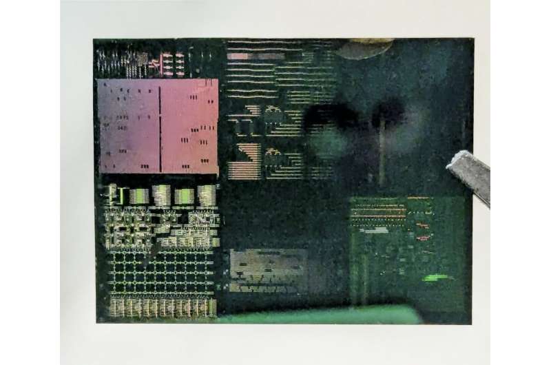
Researchers engineered a programmable photonic integrated circuit (PIC) using phase-change materials that retain their state without requiring constant electricity. This allows the chip to operate without static power consumption, unlike conventional optical chips that depend on continuous electrical input.
Photonic chips, which use light instead of electrons to process and transmit data, are already valued for their high speed, bandwidth, and efficiency in applications such as data centres, sensing, and AI hardware. However, their adoption has been limited by high power consumption, thermal issues, and a lack of flexibility.
The new design tackles these issues by combining nonvolatile materials with electrical programmability, effectively creating an optical equivalent of electronic FPGAs. This enables post-manufacturing reconfiguration, reducing the need for application-specific chip designs and shortening development cycles.
Beyond power savings, the chip also reduces device footprint and heat generation, making it more suitable for dense integration in advanced computing systems. Researchers demonstrated precise and reliable electrical control of optical circuits—an important step toward scalable and practical photonic computing platforms.
The implications are broad. The technology could accelerate AI computing, optical switching in data centers, imaging systems, and sensing applications, where energy efficiency and speed are critical. As demand for high-performance computing rises, photonic chips are increasingly seen as a key solution to overcome the limitations of traditional electronics.
While still at a research stage, the next step involves testing the chip in real-world applications and improving switching speed and endurance. If successful, this innovation could mark a turning point in the transition from electronic to photonic computing architectures, enabling scalable, low-power, and reconfigurable optical systems for future electronics.