


Can ultrathin nanomaterials be produced without complex fabrication? A laser based technique could make scalable manufacturing possible.
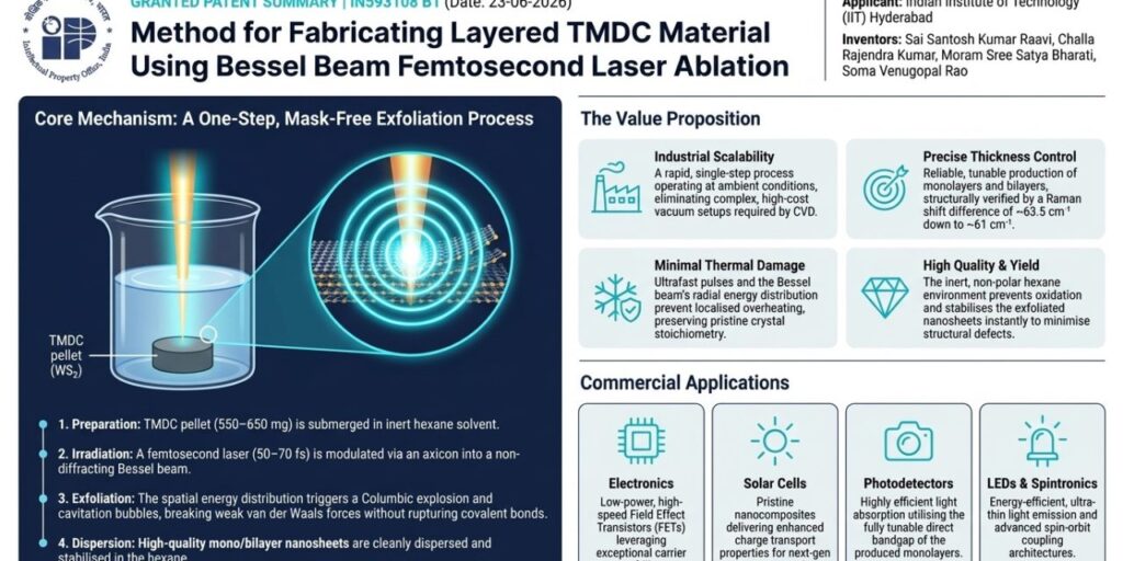
The University of Hyderabad (UoH) and the Indian Institute of Technology Hyderabad (IITH) have secured an Indian patent for a laser based technique that enables the rapid fabrication of ultrathin transition metal dichalcogenide (TMDC) nanosheets. Developed jointly by researchers from the two institutes, the method aims to simplify the production of two dimensional materials widely used in next generation electronics, photonics and sensing applications.
TMDCs have attracted significant attention because of their optical, electronic and mechanical properties. However, isolating single or few layer nanosheets from bulk material remains a major manufacturing challenge. Conventional techniques such as mechanical exfoliation, chemical exfoliation and chemical vapour deposition are often slow, expensive, chemically intensive or difficult to scale for larger production volumes.
The newly patented approach replaces these conventional processes with a femtosecond laser shaped into a Bessel beam profile. When focused onto a synthesized TMDC pellet, the ultrashort laser pulses selectively break the weak forces that hold the material’s layers together without damaging its chemical structure. This allows pristine single or multilayer nanosheets to be produced within a much shorter time while reducing process complexity.
The researchers believe the technique could provide a more practical manufacturing route for industries developing nanoscale electronic and optoelectronic devices, where material quality and production efficiency are equally important. By eliminating multiple processing steps and reducing dependence on chemical treatments, the method also offers the potential for lower production costs and improved scalability.
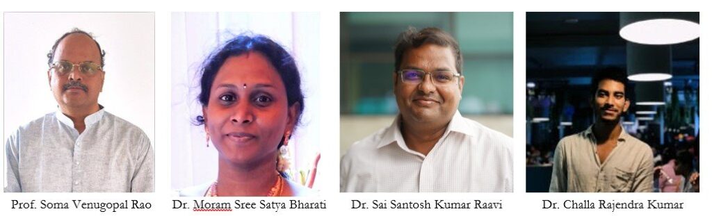
The patented technology was developed by Dr Sai Santosh Kumar Raavi, Dr Challa Rajendra Kumar, Dr Moram Sree Satya Bharati and Professor Soma Venugopal Rao through a collaborative effort between IITH and UoH. The patent marks another step towards expanding India’s capabilities in advanced materials research and laser based manufacturing technologies.