


A new technique uses a single trapped ion to create detailed maps of electromagnetic fields, helping researchers identify noise sources that affect quantum chips and sensors.
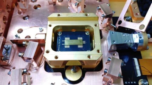
Researchers at ETH Zurich have developed a technique to produce extremely precise three-dimensional maps of electromagnetic fields above a chip surface using a single trapped ion. This method could help improve future quantum computers and quantum sensors by revealing the location of electrical noise sources which negatively impact quantum states.

The new technology is based on a chip-based Penning trap capable of transporting a single beryllium ion in all three spatial directions. In contrast to regular ion traps, which make use of oscillating radio-frequency fields, a Penning trap employs stationary electrical and magnetic fields, thus providing more freedom in manipulating ions and detecting weaker oscillating fields.
Initially, the single beryllium ion is cooled using lasers until it reaches its lowest quantum motion state. Then, the ion is transported to different locations above the chip using voltages applied to trap electrodes. The system is capable of scanning an area of 200 by 200 micrometres at heights ranging from 50 to 450 micrometres above the chip surface.
Once the ion is placed at the measurement station, the weak electric fields on the chip cause it to move in the trap. Further laser pulses measure the variations in the ion’s quantum state, allowing the scientists to compute the electric field in the vicinity. The system detected an oscillating electric field measuring only 10 nanovolts per metre in one second, while static electric fields were identified from the ion’s displacement and magnetic fields were determined from changes in its energy levels.

The group had previously developed the trap to move ions freely in three dimensions and the latest work uses that capability to scan the space above a chip and build a detailed electromagnetic map, says Doctoral researcher Tobias Sägesser.
Professor Jonathan Home said that scientists have spent more than 30 years trying to determine what causes electric field noise near quantum chips. He added that the technique could become a valuable tool for testing materials, surface coatings and fabrication methods that produce the least electrical noise, helping improve future quantum computing and quantum sensing technologies.