




Researchers have integrated terahertz generation, detection, modulation and amplification onto a single semiconductor chip, enabling compact, scalable platforms for future high-speed communications, sensing, imaging and spectroscopy applications.
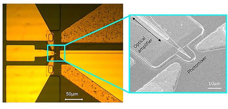
Researchers from University of California, Los Angeles have demonstrated a semiconductor chip that integrates multiple terahertz functions onto a single photonic platform, addressing one of the biggest challenges in terahertz technology—reducing the size and complexity of conventional laboratory-scale systems. The breakthrough enables terahertz signal generation, detection, modulation and amplification on one chip, paving the way for compact and scalable solutions for next-generation wireless communication, sensing and imaging.
Terahertz frequencies occupy the region between microwave and infrared light, offering exceptional bandwidth for ultra-fast data transmission while supporting high-resolution imaging and precise spectroscopy. Although these properties have made terahertz technology attractive for applications ranging from security screening and medical imaging to remote sensing and high-capacity wireless networks, existing photonics-based terahertz systems have remained bulky, expensive and difficult to manufacture at scale.
The new chip overcomes these limitations by adapting terahertz generation and detection to a photonic integrated circuit compatible with established semiconductor fabrication processes. At the core of the technology is a quantum-well PIN photonic integrated circuit architecture employing gain-enhanced interband photomixing, allowing efficient terahertz signal generation while integrating the essential optoelectronic building blocks on a common semiconductor platform. The approach significantly reduces system footprint while improving integration and manufacturability.
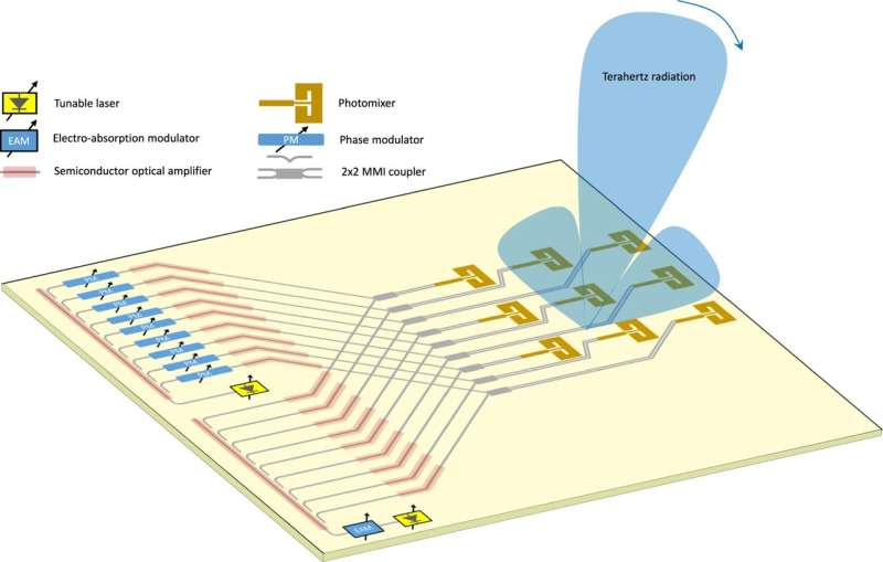
Beyond miniaturization, the integrated architecture supports future development of chip-scale terahertz phased-array transceivers capable of beam steering and adaptive operation. Such devices could enable hyperspectral remote sensing, high-speed point-to-point wireless links and advanced imaging systems without relying on multiple discrete optical and electronic components. The compatibility with industry-standard photonic manufacturing processes also increases the potential for mass production and lower deployment costs.
The development could accelerate adoption of terahertz electronics in emerging 6G infrastructure, industrial inspection, biomedical diagnostics, autonomous sensing and scientific instrumentation. By demonstrating that the critical terahertz functions can coexist on a single semiconductor chip, the research establishes a practical path toward compact, energy-efficient terahertz systems that can move beyond laboratory environments into commercial and industrial applications.

