Ansys Q3D Extractor helps engineers calculate the resistance, inductance, capacitance and conductance created by the physical structure of electronic interconnects. But can it help engineers catch electrical problems before hardware is built?
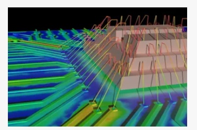
Electronic designs do not always behave exactly like their schematics. A PCB trace, IC package, connector, cable or power busbar can introduce unwanted resistance, inductance and capacitance simply because of its physical shape, size, material and position relative to other conductors.
Ansys Q3D Extractor is designed to analyse these effects. The software performs two-dimensional (2D) and three-dimensional (3D) quasi-static electromagnetic simulations to extract frequency-dependent resistance, inductance, capacitance and conductance, collectively known as RLCG parameters, from physical interconnect structures.
This helps engineers understand how the physical implementation of an electronic design affects its electrical behaviour. The extracted parameters can also be converted into equivalent SPICE models for further circuit and signal-integrity analysis.It is used for applications ranging from IC packages, connectors and PCBs to high-power busbars, power converters and electric-drive systems. Instead of treating a conductor as an ideal connection, engineers can analyse the electrical behaviour introduced by the actual geometry of the structure.
What Can You Do With This Tool?
It focuses on one important engineering question: what electrical behaviour is created by the physical structure of an interconnect?
1. Extract Hidden Parasitic Parameters: Electronic conductors introduce parasitic effects that may not appear in a circuit schematic. A long trace can introduce inductance, closely spaced conductors can create capacitance, and resistance can change with frequency because of effects such as skin and proximity effects.The tool calculates frequency-dependent RLCG parameters directly from the physical model.This allows engineers to identify electrical effects caused by the geometry of packages, interconnects and power structures before producing hardware.
2. Analyse Packages and High-Speed Interconnects:Advanced IC packages and high-speed connectors contain increasingly dense interconnect structures. At higher frequencies, the electrical behaviour of these structures can significantly affect signal integrity.It can analyse the parasitic behaviour of packages, connectors and PCB interconnects and generate models that can be used in wider signal-integrity simulations.Instead of manually estimating parasitic values, engineers can extract them from the geometry of the actual structure.
3. Design High-Power Electronics:The same physical effects also matter in power electronics.Busbars and power-converter connections can introduce unwanted resistance and inductance. These parameters can affect switching behaviour, losses and the overall electrical performance of the system.The tool can therefore be used for high-power busbars, electrical power-distribution systems, power converters and electric-drive applications.
4. Study Frequency-Dependent Behaviour:A conductor does not necessarily behave the same way at every frequency.It includes quasi-static electromagnetic solvers that can account for frequency-dependent effects, including skin effect, proximity effect, dielectric loss and ohmic loss.This gives engineers a more realistic view of how an interconnect behaves as operating conditions change.
5. Generate Circuit Models:After extracting the parasitic parameters, the tool can automatically generate equivalent circuit models.These models can be used in circuit and signal-integrity workflows, helping engineers connect electromagnetic analysis with wider electronic-system simulations.This is particularly useful when the physical geometry and the circuit behaviour need to be analysed together.It also includes features designed to make electromagnetic extraction more practical for larger engineering projects.
It automatically refines the simulation mesh in the most critical regions of a model through automatic adaptive mesh refinement, improving accuracy without requiring engineers to manually apply an extremely detailed mesh across the entire structure.
The software also supports both 3D parasitic extraction for complex physical structures and 2D extraction for applications such as cables and transmission lines. Engineers can select different extraction approaches depending on whether they need to analyse resistance, inductance, capacitance or complete RLCG behaviour. In addition, the extracted models can be used for power and signal integrity analysis, helping engineers understand electromagnetic effects in high-speed electronic circuits and power-electronics systems. Together, these capabilities enable engineers to move efficiently from a physical interconnect model to accurate electrical parameters and circuit models while reducing dependence on simplified assumptions.One engineer discussing power-module analysis described using this tool said that “it is super useful, specifically for calculating loop inductance, showing how the software is used to investigate real parasitic effects in power-electronics structures”.
What’s New?
The recent development of Q3D Extractor is 2026 R1, which was officially released on March 11, 2026.It is focused on improving how extracted electromagnetic information moves through the wider electronics-design workflow.One important recent update introduced ohmic-loss evaluation at contact-resistance boundaries. This can help engineers analyse losses associated with electrical contact regions, which can become important in power and interconnect structures.
Another significant addition is the ability to create a causal RLGC netlist workflow between Q3D and HFSS 3D Layout. Earlier workflows could require engineers to handle extracted electromagnetic data separately when moving between analysis environments. The newer capability makes it easier to use Q3D’s extracted parasitic information in layout-level analysis.
Recent releases have also improved mesh-refinement error calculations for AC resistance and inductance extraction, helping engineers evaluate and refine simulations involving frequency-dependent RL behaviour.These improvements build on earlier solver developments. The 2024 R1 release introduced a distributed-memory solver capability and a new AC-RL solver designed for substantial packages.Together, these updates show how Q3D is evolving beyond simply calculating parasitic values. The software is becoming more closely connected to larger signal-integrity, packaging and electronics-analysis workflows.For engineers, the important change is not just faster simulation. It is the ability to move more easily from physical geometry to extracted parasitics and then into wider electronic-system analysis.
How to Start With the Free Version
Ansys offers a free Ansys Electronics Desktop Student version that includes Q3D Extractor for educational use.The student edition allows users to model, mesh, solve and post-process Q3D simulations, making it possible to learn parasitic extraction and experiment with smaller electronic structures.However, the free version has limitations.For Q3D Extractor, mesh sizes are limited to:
- 64,000 3D volume elements
- 8,000 3D surface elements
- 2,000 2D triangles
The student version also supports local solving only and limits high-performance computing to four cores. Geometry export is not supported, while geometry import is limited to DXF and STEP formats.These restrictions make the free version better suited to learning, education and smaller models rather than large commercial simulations.
The commercial version is designed for engineers working with larger packages, complex interconnects and demanding power- and signal-integrity problems.Ansys Q3D Extractor addresses a problem that becomes increasingly important as electronics become faster, denser and more power intensive. A schematic can describe what an engineer intends to connect, but it does not always reveal how the physical structure of those connections will behave.Q3D Extractor fills that gap by turning physical geometry into electrical parameters.
By extracting resistance, inductance, capacitance and conductance from packages, PCBs, connectors, cables and power structures, the software helps engineers identify parasitic effects before they become hardware problems. Its recent improvements in loss analysis, RLGC workflows and solver technology further extend its role in modern electronics design.
For engineers working with advanced packaging, high-speed electronics or power systems, the tool’s real value lies in one simple capability: revealing the electrical behaviour hidden inside the physical design.
| Software | Free access | Platform | What you get for free |
| Ansys Electronics Desktop Student | Free for eligible educational use | Windows | Access to Q3D Extractor and other electronics simulation tools, with mesh, import, HPC and workflow limitations |
| Ansys Electronics Desktop Commercial | Commercial licence | Windows | Larger-scale simulation capabilities and commercial engineering workflows |
| Q3D Extractor | Included in the student edition with restrictions | Windows | 2D and 3D parasitic extraction for smaller educational projects |
How Q3D Extractor Fits Into the EDA Workflow
Electronic design automation covers a broad range of activities, including schematic design, PCB layout, circuit simulation, electromagnetic analysis, IC design and manufacturing preparation.
Q3D Extractor occupies a specialised position within this workflow.
It does not replace PCB-design software or schematic-capture tools. Instead, it analyses the electromagnetic behaviour created by the physical structures used to implement an electronic design.
The software focuses on extracting parasitic resistance, inductance, capacitance and conductance from structures such as IC packages, PCB interconnects, connectors, cables and power busbars.
This allows engineers to connect physical design decisions with electrical performance and use the extracted information in wider circuit, signal-integrity and power-electronics workflows.
For more information, click here.