

Huawei’s new semiconductor architecture could raise transistor density while reducing power and heat, potentially improving smartphone processor performance amid limited access to advanced chipmaking tools.
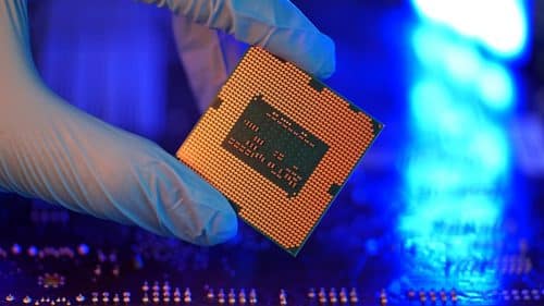
Huawei has published new measurements for its Tau Scaling Law-based architecture, reporting that the approach could increase transistor density while reducing power consumption and heat in the upcoming Kirin 9030 Pro smartphone processor. The findings highlight an alternative path to improving chip performance as access to advanced semiconductor manufacturing equipment remains constrained.
The architecture is based on LogicFolding, Huawei’s approach to arranging chip circuitry vertically rather than relying entirely on conventional two-dimensional layouts. By stacking circuit layers, the company aims to shorten the distance signals travel between processing components.
Huawei says this can reduce energy losses in neural processing units, graphics processing units and digital signal processors, which are among the components contributing to smartphone processor power consumption and thermal output.
According to the published measurements, the new design is expected to deliver about 55% higher transistor density than the Kirin 9030 Pro, while also reducing power consumption by as much as 30% for some workloads. The approach combines vertical integration with thermal planning to distribute heat more effectively across the chip.

Huawei reportedly reduced power density by folding and repositioning modules along paths where heat can escape more easily. This is intended to address one of the major challenges associated with increasing transistor density: maintaining performance without creating excessive thermal loads.
The technology is particularly significant because Huawei is developing it under restrictions affecting China’s access to some advanced chipmaking tools. The company’s Tau Scaling Law proposes increasing transistor density without depending entirely on cutting-edge extreme ultraviolet lithography.
Huawei has also suggested that LogicFolding could eventually achieve transistor densities comparable with those associated with 1.4-nanometre manufacturing processes. Its latest production-related measurements are intended to support that direction.
The work points towards broader developments in three-dimensional chip integration, potentially encouraging new approaches to semiconductor materials, packaging and manufacturing. For smartphones, the combination of greater density, lower power and improved thermal behaviour could help support increasingly demanding AI workloads.