




Agentic AI can now guide X-ray scans of microelectronics using natural-language instructions, combining real-time image reconstruction, autonomous navigation, and AI-based feature segmentation.
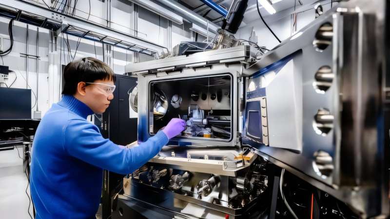
Researchers at Argonne National Laboratory have demonstrated an agentic AI system that can autonomously guide X-ray imaging of microelectronics, potentially changing how semiconductor devices are inspected and analysed. The system, developed under the SYNAPS-I project, allows researchers to describe an imaging task in natural language rather than manually operating complex beamline controls.
At the core of the system is ptychography, an X-ray imaging technique that captures overlapping diffraction patterns and computationally reconstructs them into high-resolution images. During experiments, ultrabright X-ray beams can generate millions of images within a few hours. SYNAPS-I uses the PtychoFM AI model to reconstruct these images in real time, reducing analysis that could otherwise take hours or days to seconds.
The newer agentic layer adds autonomous decision-making to this imaging pipeline. A researcher can issue instructions such as mapping a region or examining an area at higher resolution. The AI interprets the request, examines reconstructed images, identifies relevant features, determines where to scan next, and progressively narrows the search.
This is particularly useful for region-of-interest detection in semiconductor structures, where the target feature may be small and its location can vary between samples. Instead of relying on a fixed sequence of programmed movements, the multimodal AI agent evaluates each newly generated image and decides its next action. Low-risk operations can be performed autonomously, while actions involving greater uncertainty can require human approval.
The researchers also integrated Meta’s Segment Anything Model 3 (SAM3) for image segmentation. This enables the system to isolate and label features in reconstructed images, giving the agent additional visual information for navigation and analysis.
In a demonstration using an integrated-circuit sample, the AI was instructed to locate an interface between two regions. Starting from a point inside the device, it repeatedly scanned, analysed, segmented, and navigated until it identified the required region, after which it could initiate a higher-resolution scan.
The approach could eventually support self-driving microscopes, closed-loop experiments, and automated semiconductor defect detection, moving X-ray inspection from passive imaging towards adaptive, AI-controlled analysis.

