





How can chipmakers model materials, detect defects and refine fabrication processes faster? A tool can now target engineering bottlenecks across chip development and manufacturing.
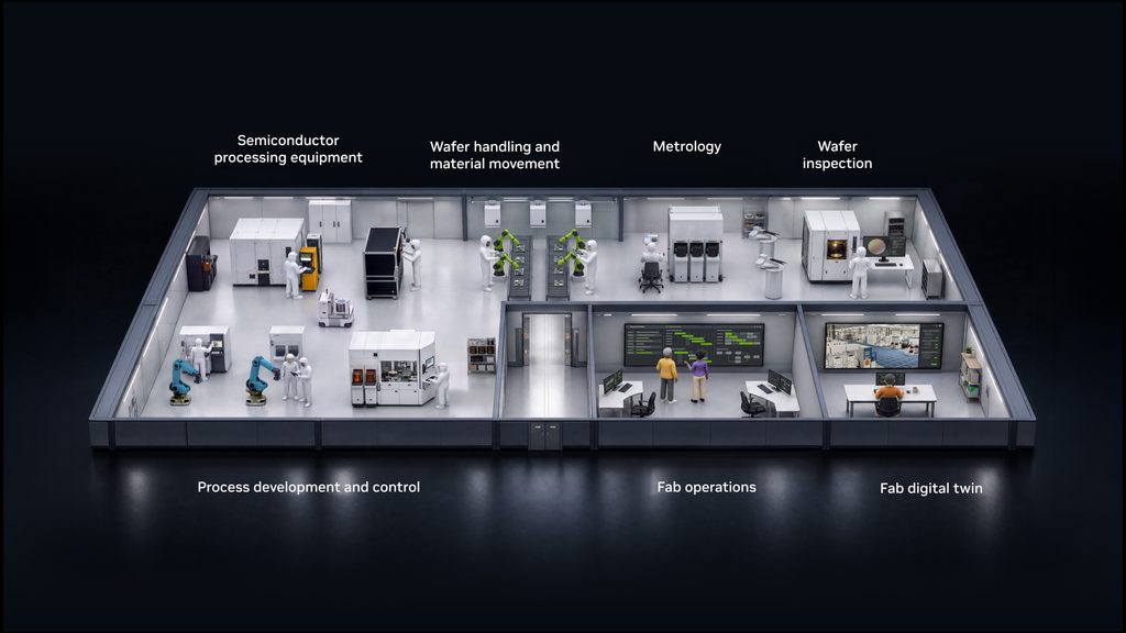
NVIDIA is expanding its accelerated computing portfolio for semiconductor engineering, helping companies speed up materials simulation, chip design, wafer-process modelling and inspection. Its CUDA-X libraries and AI software are intended to help engineers analyse complex processes and evaluate changes before applying them to semiconductor production.
Faster simulations and image processing could help chipmakers shorten development cycles, investigate defects and improve manufacturing yields. By modelling material behaviour and fabrication processes, engineers can assess design options and identify potential issues before committing to costly fabrication runs or process changes.
The latest addition, NVIDIA cuPotential, is available in early access. It provides GPU-accelerated functions for modelling interactions between atoms and molecules, allowing developers to build AI agents that run and refine materials simulations. In early-access testing, it accelerated existing GPU-optimised workflows by an additional two to three times. Synopsys is among its early adopters.
Other libraries address different semiconductor engineering tasks. NVIDIA cuEST supports electronic-behaviour modelling, while cuDSS accelerates engineering simulations. Synopsys has reported potential speedups of up to 30 times in QuantumATK results using cuEST and 12 times in S-Device benchmarks using cuDSS.
For wafer fabrication, Lam Research plans to integrate NanoVDB, an open-source library for processing 3D data, into its SEMulator3D process-modelling platform. The integration is expected to accelerate selected wafer-etch simulations by up to 30 times. Such modelling can help engineers study how fabrication steps affect semiconductor structures before implementing process changes.
Chip inspection is another application. KLA reported that an image-processing kernel using NVIDIA NPP, a GPU-accelerated image-processing library, performed up to 50 times faster than earlier CPU implementations. Faster image analysis can help engineers process inspection data used to identify defects and assess manufacturing quality.
The technology is also being applied to advanced packaging, semiconductor testing and factory optimisation by companies including Cadence, Teradyne and Applied Materials. NVIDIA NPP is available through the CUDA Toolkit, NanoVDB is open source, and cuPotential remains in early access.
Click here for the official announcement.

